Next-generation networks may benefit from SOAs
Martin Young
As the demand for bandwidth continues to increase, optical networks are expanding from the long-haul backbone to the metropolitan and potentially the local access markets. Related cost constraints mean that optical-system designers must find compact, low-cost alternatives to existing component solutions.
In its simplest form, the semiconductor optical amplifier, or SOA, can be used to boost an optical signal that has weakened during propagation through a fiber. Historically, this has been done using an erbium-doped fiber amplifier (EDFA) due to its lower noise, higher output power, and negligible crosstalk between channels. Although SOAs may never replace EDFAs, their small size and ease of integration, as well as their nonlinear properties make them a promising candidate for next-generation optical networks. An EDFA contains lengths of doped fiber, one or more pump lasers, couplers, and isolators, resulting in a module the size of which can vary between that of a deck of cards and a videocassette.
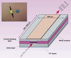
In contrast, an SOA is a discrete component housed in a butterfly package with a footprint of less than one square inch (see Fig. 1). Furthermore, SOAs are fabricated using the well-defined indium phosphide-based processing technology developed for many of the lasers and detectors in use today. This technology has allowed the SOA to be integrated on-chip with passive waveguides, leading to devices with all-optical functions such as switching, adding and dropping of a channel, or wavelength conversion. Using currently available manufacturing techniques, thousands of these chips can be fabricated at the same time on a single substrate, and with advanced packaging platforms high yields will ultimately lead to module costs low enough to facilitate system-wide implementation.
Basic principles
An SOA is essentially a semiconductor laser, but care is taken to prevent internal feedback so that an optical signal travels through the device only once and emerges intensified at the other end. As electrical current is applied to the device, electrons within the semiconductor gain medium are placed in an excited state. These excited electrons become stimulated by the incoming optical signal and return to the ground state. This stimulated emission results in another photon with characteristics matching the photon that caused the emission in the first place. This process continues as the signal travels through the device until the photons exit together as an amplified signal. The gain medium of the device can be prepared with either a bulk or multiple quantum well (MQW) structure. The peak wavelength of this gain can be engineered to vary within a very large range of between 1300 and 1600 nm depending on the composition of the epitaxially grown material.
To prevent any significant oscillation from building up in the SOA, a facet reflectivity of less than 0.01% is necessary. Antireflection coatings can effectively drop reflectivities to the required levels when applied to both facets, but their thickness tolerances are often too tight for high-volume manufacturing. Typically, these coatings are used in conjunction with other methods to reduce the facet reflectivity. One method is to tilt the optical waveguide with respect to the facet normal by 5° to 10°. Any light reflected from the facet will propagate away from the waveguide, and although some light may couple back in, this method typically can reduce reflectivities by an order of magnitude. Another method that can effectively reduce reflectivities is to terminate the optical waveguide prior to the facet. This technique, known as a window, allows the optical mode to spread out before it reaches the facet, and continue to spread as it propagates back toward the waveguide, resulting in only a fraction of the light being coupled back into the waveguide. Since this method requires additional processing steps and a fairly tight control on the length of the window section, it is less widely used.
Performance issues
The small-signal gain of an SOA can be as high as 35 to 40 dB, and the 3-dB bandwidth of this gain is typically between 45 and 60 nm, depending upon whether a bulk or MQW active region is used, with the latter giving a wider bandwidth. As the input optical power increases, the electron consumption, which resulted in stimulated emission, increases rapidly until the demand outpaces the supply. At this point the optical gain begins to saturate, and this limits the maximum output power of the SOA. Increasing the electron supply with more current increases the maximum output power, but just as there is a limit to how hard a diode laser can be driven before thermal rollover, so too is there a limit for an SOA. With improvements in device design and the quality of semiconductor growth, saturation output powers approaching 100 mW have been obtained.
Much of the fiber installed today does not preserve the state of polarization, and therefore any in-line component should be polarization insensitive. The EDFA is inherently polarization insensitive due to the symmetrical nature of the fiber core, but a traditional SOA will provide different gains for TE and TM polarizations due to its rectangular cross section. Initially, this problem was overcome by simply fabricating a symmetrical waveguide in the semiconductor. To maintain the single-mode characteristics, however, the width of the waveguide needed to be less than 0.5 µm, and this dimension is extremely difficult to control in a manufacturing environment. In the past several years, more manufacturing-friendly methods have been demonstrated with TE/TM gain differentials of less than 0.5 dB. A common theme of these methods is the application of various strains to either a bulk or MQW active region, which typically results in enhancing the TM gain to equal that of the TE mode.
One of the toughest challenges to manufacturers of SOAs will be to reduce the noise figure of the device, which is the amount of degradation in the signal-to-noise ratio caused by the amplification process. As the optical signal travels through the SOA, the stimulated emission is accompanied by spontaneous emission. This will add photons of random phase and polarization, thereby degrading the clarity of the signal. With device optimization, the noise figure of the semiconductor chip can be kept low, and values as low as 4 dB, or equal to that of an EDFA, are obtainable. At the module level, however, coupling losses between the single-mode fiber and waveguide, which results from the highly divergent and asymmetrical far-field profile of the conventional SOA, leads to an increase of the noise figure by as much as 3 to 6 dB. Conversely, EDFAs see very little increase in noise figure due to a low loss fiber-to-fiber coupling. For SOAs to be used effectively in optical networking, the coupling efficiency must be optimized. This is achieved most commonly by tapering the waveguide in both the vertical and horizontal directions such that the waveguide narrows to a point. This technique can lead to an output-mode profile that more closely matches a single-mode fiber, resulting in much higher coupling efficiencies and lower noise figures.
Applications
Originally designed to be an in-line amplifier until the advent of the EDFA, the SOA has received renewed interest due to the penetration of optical networking into the metro and access layers. In these applications, a compact, low-cost amplifier that consumes little power will be needed to compensate for losses resulting from switching and routing of the optical signal. Semiconductor optical amplifiers can be used as a booster amplifier after the transmitter. Recently, tunable lasers have received considerable attention as a source for dense wavelength-division multiplexing (WDM) systems. Typically, output powers of these transmitters are very weak due to the large tuning range. By placing an SOA module on the same driver board as the transmitter, much greater output powers can be launched. Conversely, placing the amplifier in front of the detector to boost the received power can also increase transmission distance.
Amplification may soon be required outside the widely used long-haul wavelength range of 1550 nm where EDFAs dominate. Short-haul systems that operate in the 1310-nm range and previously had no need for amplifiers may soon require them as bit-rate and routing functions increase. Currently, the SOA appears to be the most viable choice for this application, since fiber amplifiers in this wavelength range are not well developed.
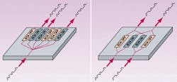
Fast switching speeds of less than a nanosecond, and high extinction ratios of greater than 50 dB have lead to the use of SOAs as optical gates, and when integrated with passive waveguides these gates can be used to form switching matrices (see Fig. 2). The potential to compensate for optical losses, while at the same time executing the switching function, is a unique feature of SOA-based switches.
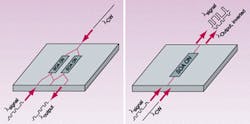
Perhaps one of the largest potential applications for SOAs is that of all-optical wavelength conversion. As the number of channels increases in WDM networks, there is an increased probability that transmitters at different locations will send signals to the same destination using the same wavelength. To avoid such wavelength contention, converters are required to transfer signals from one carrier wavelength to another. Currently, this function is accomplished using optical-electrical-optical (OEO) conversion in much the same way that signal amplification was done before optical amplifiers. A receiver first converts the input optical signal to electronic form, which is then reshaped and retimed, and this electronic signal is used to drive a transmitter at the new wavelength. The disadvantages of OEO converters, is their inherent dependence on the data rate and format of the incoming signal, as well as the overall complexity and high cost of the receiver-transmitter pair. All-optical wavelength converters are more compact, less complex, and independent of the input-signal format. Two methods of converting wavelengths using SOAs are cross-gain modulation and cross-phase modulation (see Fig. 3)
Cross-gain modulation (XGM) is a very simplistic approach to wavelength conversion, since only a discrete SOA is needed. In this approach, a high-power data signal of one wavelength, and a DC signal of lower power and at a second wavelength, are coupled into the SOA. The strong signal saturates the gain of the amplifier and thus transfers the inverse of its data onto the DC signal. Unfortunately, although this method has demonstrated extremely fast wavelength conversion with speeds of 100 Gbits/s, it has come at the cost of wavelength instability, or chirp.
The cross-phase modulation (XPM) converter is more complicated to fabricate but has improved performance such as reduced chirp, a larger extinction ratio of the converted wavelength, and suppressed amplified spontaneous emission. For this device, two SOAs are integrated with passive waveguides to form an interferometer. The DC signal is split and passes though each of the SOAs. The data signal enters one of the SOAs, depleting the carrier density, which subsequently changes the refractive index. This results in a phase shift of the DC signal through that SOA, and after passing through the interferometric stage of the device, the phase modulation is converted into intensity modulation.
A viable solution
The challenge for next-generation optical-network designers is to provide service providers a profitable solution to expand into the metro and local access markets. To accomplish this, the networks will need to be more flexible with lower-cost components providing increased functionality. The SOA and integrated devices based on this technology, have demonstrated many all-optical functions including amplification, switching, and wavelength conversion. The current challenges include improving fiber-to-waveguide coupling, exploring integration platforms such as hybrid integration, and implementing high-volume manufacturing techniques to drive down cost. Since these challenges are far from insurmountable, however, the potential for compact, low-cost modules makes the SOA a technology to watch.
MARTIN YOUNG is vice president of optoelectronics at Optical Crossing Inc. 411 N.Central Ave., Glendale, CA 9203; email: [email protected].


