Waveguide amplifiers compensate passive optical component losses
JULIAN BRISTOW
Erbium-doped waveguide amplifiers exploit planar technology to implement many amplifier functions, both active and passive, on a single chip.
The widespread deployment of dense wavelength-division multiplexing (DWDM) systems was facilitated by the development of high-power erbium-doped fiber amplifiers (EDFAs). As DWDM systems extend into the metro area, EDFAs will also be used in the core of the network if their costs can be justified. In both long-haul and metro networks, additional needs exist for optical amplifiers at the edge of the network, or adjacent to passive components that introduce localized loss.
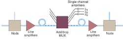
In DWDM systems, routing components such as switches and optical add/drop multiplexers (OADMs) can add losses that are small, but that may not be tolerated by the optical power budget for the system. Amplification can overcome these losses. An example would be to compensate for the loss of an OADM (see Fig. 1).
Different wavelengths in a network can be routed to different destinations, and it is advantageous to be able to adjust the power level of each wavelength independently. One way to accomplish this is to provide amplification for each individual wavelength.
Conventional DWDM EDFAs, often designed to provide uniform gain over the full C-band, can be used to amplify individual wavelengths. The EDFAs are, however, often optimized for higher gain and power than are needed for single-channel applications, and may not be cost effective. Single-channel amplifiers, in contrast, are simple, non-gain-flattened amplifiers. When used in a DWDM system, they allow the gain of each channel to be optimized, and can also allow functions such as optical attenuation to be implemented. Single-channel amplifiers can also be used to replace existing functions; for example a number of single-channel amplifiers could replace a fixed-gain WDM amplifier combined with an array of variable optical attenuators.
Requirements for single-channel amplifiers
To compensate for the loss of routing components, only moderate gains of 8 to 10 dB are needed. For other applications in which the loss over a partial span of fiber must be compensated, higher gain is necessary. Gains of 10 to 15 dB across the C-band allow flexibility in amplifier placement. Output powers need only be modest when amplification is provided on an individual wavelength basis, and 10 dBm is adequate for many applications.
Cost is important. Because single-channel amplifiers represent only one of several possible system solutions, they must be competitive with schemes in which a broad range of wavelengths is amplified and separate provisions are made for adjustment of individual channel power.
Noise is also an important consideration. Optical amplifiers degrade the optical signal-to-noise ratio of a link to differing extents, and different applications in a network have varying degrees of sensitivity to noise. The degradation of the signal-to-noise ratio caused by a single amplifier is quantified by the noise figure. Many applications require noise figures to be no higher than 5 or 6 dB.
Power dissipation is also a critical factor. Power dissipations of less than 1 W are desirable for single channel amplifiers. System manufacturers seek ways to increase the number of channels in DWDM systems, but there are limits on the power dissipation that can be tolerated in a rack of network equipment. Size is also an important parameter, because many wavelengths must be amplified in the same physical space, and board space is at a premium for DWDM systems.
In most applications, single-channel amplifiers must incorporate both an input and an output monitor. The monitors tap a small portion of the input and output signals to enable monitoring and control of the operation of the amplifier. In addition, optical isolators must be provided for many applications to render the amplifier immune to reflections elsewhere in the system.
Some single-channel amplifier solutions are able to incorporate only some of these features and the cost of providing these functions in a system must be taken into account when considering the different amplifier options.
Erbium-doped waveguide amplifiers
One solution to the problem of providing compact, low-cost single-channel amplification is to use erbium-doped waveguide amplifiers (EDWAs). These devices use erbium to provide amplification in the same way as today's EDFAs, but exploit planar technology to implement many amplifier functions, both active and passive, on a single chip. Since the cost of producing the chip scales favorably with the number of components on the chip, this solution can be cost effective in many applications. The chip can then be packaged with standard single-mode fiber similar to any other integrated optical device, and the amplifier can then be incorporated in a network (see Fig. 2).
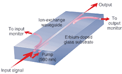
The basic gain element is implemented by using photolithographic processes to define a region on the surface of an erbium-doped glass substrate. The refractive index of the uniformly doped substrate is increased using an ion-exchange process to form a waveguide.
The ion-exchange process can be tailored to produce a mode size that optimizes the efficiency of the device, and that provides a waveguide with a high degree of symmetry to minimize variations in gain with polarization. The glass must be chosen carefully to allow high doping levels, and hence high gain, without producing clustering effects in the erbium. Clustering can reduce the efficiency and degrade the noise characteristics of amplifiers. With careful selection of glass and erbium levels, peak gains in excess of 3 dB/cm can be realized. To provide gain, the waveguide amplifier must be pumped, which is accomplished by end-pumping the waveguide, often at 980-nm at which high-power pumps are readily available at low cost.
A basic amplifier element consists of a pump laser, an ion-exchanged waveguide in the doped glass substrate, and a pump/signal combiner. The pump/signal combiner is a waveguide device that can be fabricated on the same substrate as the gain element, and is optimized to minimize the signal loss for the 1550-nm input, while maximizing the 980-nm power coupled into the amplifier.
The EDWA can be designed to use pump power efficiently. Careful optimization of the waveguide geometry can produce waveguides that provide gains as high as 24 dB with pump powers little higher than 100 mW. Output powers in excess of 10 dBm can also be realized.
In addition to the pump/signal combiner couplers, additional waveguide structures can be made that tap a small fraction of the input and output signals and route the tap signal to a detector located close to the chip. In this way taps for input and output monitors can be incorporated with minimal incremental cost.
Pump lasers and packaging
One way to reduce power dissipation is to use uncooled pump lasers. In a standard pump laser, the thermoelectric cooler can account for 80% of the total power dissipation. Elimination of the cooler provides one path to lowering the power dissipation, however pump lasers must be chosen carefully to ensure acceptable reliability at useful power levels. Fortunately, uncooled pump lasers that provide sufficient power for waveguide amplifiers have become available. Reliable operation now can be expected for amplifiers with output powers in excess of 10 dBm and with package temperatures as high as 70°C.
To be useful in a system, a waveguide amplifier must be provided with input and output fibers. Many schemes are in use for pigtailing integrated optical devices. To ensure the highest possible reliability, however, epoxy-free packaging is preferred. High optical-power densities exist in the region where the pump laser is launched into the chip, giving rise to the possibility of oxidizing out-gassed components if any epoxies are used. This oxidation can subsequently degrade the performance of the amplifier. In contrast, laser-welding techniques, which are often used to package semiconductor lasers, can be extended to the packaging of integrated optical components. Laser-welded packages can have excellent long-term stability and eliminate the use of epoxy.
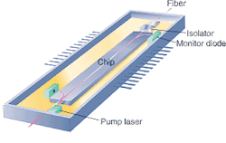
Planar technologies, like fiber-based technologies, cannot readily implement optical isolators. These must be added as separate components in the packaged amplifier. Because the package already incorporates chip-level components, it is relatively straightforward to incorporate unpackaged optical isolators and other components, such as pump lasers, using the same technology as is used to package the amplifier chip. This can result in lower cost than if fully packaged or pigtailed components were used (see Fig. 3).
Julian Bristow is vice president of marketing and business development at Northstar Photonics, 6464 Sycamore Ct., Maple Grove, MN 55369; e-mail: [email protected].