PHOTOLITHOGRAPHY: ‘Align-and-shine’ easily patterns optical-fiber tips

About three years ago, researchers at Vrije Universiteit (Amsterdam, The Netherlands) created a tiny interferometric sensor that fit on the end of an optical fiber; the so-called “fiber-top” sensor consisted of a micromechanical cantilever that would deflect or vibrate, reflecting light from the fiber back into the fiber in proportion to the cantilever’s deflection.1 Micromachined out of the optical fiber itself, the cantilever detects deflections to a 0.1 nm sensitivity; the sensor can be used in tight spaces, as well as in hostile or electrically conductive environments.
While the cantilevers can be made by carving them out of a fiber tip using an ultrafast laser, the researchers have recently come up with an easier way. Called “align and shine” photolithography, the new technique is potentially useful not only for fabricating cantilevers cantilevers, but for making many other types of fiber-end micro-optical, mechanical, or chemical sensors.2 Another benefit of the align-and-shine technique is its rapidity, which makes possible large-scale fabrication of devices.
In align-and-shine photolithography, a photomask on the end of a UV-transmitting multimode optical fiber (the “mask” fiber) is aligned and brought into contact with the photoresist-coated end of the target fiber, allowing the photomask pattern to be transferred to the photoresist. What makes the process unique is that the alignment is done using only a commercial optical-fiber fusion-splicing machine (no splicing is done, though). Years of development have made commercial fusion splicers into very capable and easy-to-use image-based active fiber aligners; the align-and-shine process thus becomes quick, straightforward, and inexpensive.
Test pattern
The ends of the 230-µm-diameter experimental fibers were cleaved with a commercial optical-fiber cleaver, producing surfaces flat and perpendicular to the fibers’ optical axis to less than 0.5°, which is fine for the align-and-shine process, according to Davide Iannuzzi, the project’s group leader.
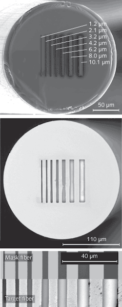
The photomask was fabricated on the end of the mask fiber by first coating it with a 100 nm layer of silver, then creating a pattern by selectively removing the layer with a focused ion-beam milling machine. The test pattern on the prototype consisted of seven stripes of different widths ranging from 1.2 to 10.1 µm.
The photoresist was deposited onto the end of the target fiber by dipping—an approach that, although workable for the prototype, is not optimum, says Iannuzzi. “This method is giving layers that are way too thick,” he notes. “The simplest solution is, in our opinion, to use spray photoresist. We did not do that for a very simple reason: the use of spray photoresist produces fumes that might be not too healthy; therefore, it would be better to use those sprays under negative-pressure hoods, which are not available in our lab. Another possible solution (but more challenging) is to use dipping (as already described in the paper) and, before backing, thin it by spinning the fiber along its principal axis (similar to what is done with conventional photolithography on large wafers). It is then necessary to build a dedicated holder for the spinner . . . but this is just a mechanical problem.”
The two fibers were then aligned on the splicer and UV light sent through the mask fiber for about 10 s. After developing, the target pattern was compared to the mask pattern (see figure), showing a resolution of about 2 µm. The researchers repeated the experiment using two fibers of differing diameters (230 and 125 µm); the fusion splicer allowed them to align the fibers as precisely as if they were the same diameter.
To make a real fiber-top microdevice, such as a microelectromechanical-systems (MEMS) mechanism or a microlens, the photolithographic process would be carried further, with etching (see www.laserfocusworld.com/articles/292405), perhaps deposition of further materials, and probably additional rounds of align-and-shine lithography. “We are confident that we can improve the resolution by a factor of two with a better photoresist-deposition technique, and that we can probably go submicron using, for example, photo or thermoplastic nanoimprinting,” says Iannuzzi.
Other uses
In addition to MEMS and micro-optics, Iannuzzi sees other potential applications. “For example, a group at Harvard has recently described a very interesting surface-enhanced Raman-scattering (SERS) detection device based on the fabrication of metallic nanoantennas on the tip of an optical fiber.3 If we can push the resolution of align-and-shine photolithography to the submicron regime, we might be able to fabricate those optical antennas with a cheaper process,” he says. “In general, we are confident that the align-and-shine technique will soon attract the attention of scientists who, in the past, have put a nice idea in the drawer because there was no technique to make arbitrary patterns on the top of an optical fiber. Those ideas can now be taken out of the drawer.”
REFERENCES
- D. Iannuzzi et al., Appl. Phys. Lett. 88, 053501.
- A. Petrušis et al., J. Micromech. Microeng. 19 (2009) 047001.
- Elizabeth J. Smythe et al., Nano Lett., 2009 (3), p. 1132.
About the Author
John Wallace
Senior Technical Editor (1998-2022)
John Wallace was with Laser Focus World for nearly 25 years, retiring in late June 2022. He obtained a bachelor's degree in mechanical engineering and physics at Rutgers University and a master's in optical engineering at the University of Rochester. Before becoming an editor, John worked as an engineer at RCA, Exxon, Eastman Kodak, and GCA Corporation.
