Multimode Fiber-Optic Components: Multimode silicon photonics gains WDM-compatible multiplexer
While high-bandwidth optical communications as well as chip-based integrated silicon photonics architectures typically comprise single-mode fibers working in concert with single-mode wavelength-division multiplexing (WDM) devices, multimode communications (and multimode integrated photonics) over multimode optical fibers are continuing to progress via space-division multiplexing in multicore fibers and through mode-division multiplexing in few-mode fibers.
Because WDM devices demand low-crosstalk performance to enable error-free transmission of information carried on closely spaced wavelengths multiplexed onto a single-mode fiber, multimode WDM devices—with their typically high intermodal crosstalk—have long precluded the demonstration of true multimode mode-division-multiplexing (MDM)-based communications. But Michal Lipson’s group at Cornell University (Ithaca, NY) working with Keren Bergman’s group at Columbia University (New York, NY) have together demonstrated microring-based, on-chip WDM-compatible MDM with both low modal crosstalk and loss, dramatically improving the prospects for future multimode silicon photonics.
Multimode multiplexing microrings
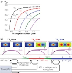
To engineer the multiplexer, a series of photonic microrings enable selective phase coupling to different spatial modes for a particular wavelength. The multiplexer design begins with a 250-nm-tall waveguide that varies in width from 450 nm to 930 nm to 1.41 μm (with each section connected by adiabatic tapers). The three sections of this varying-width waveguide sit in close proximity to three ring-resonator structures that are engineered to selectively couple to specific spatial modes in the waveguide; for example, the TE0, TE1, or TE2 mode of a 1550 nm signal (see figure). In each section, the dimensions of the multimode waveguide and ring structures determine which mode is coupled into which microring according to phase-matching conditions and coupled-mode analysis.
Optimized for minimal insertion loss and crosstalk between modes, the microring structures are also designed for a resonance linewidth of at least 15 GHz to enable 10 Gbit/s data transmission with minimal signal degradation. A heater on top of each microring further fine-tunes the resonance to align with the desired WDM channels or provide controllable and tunable coupling to certain wavelengths.
When arranged in a multiplexing-demultiplexing architecture, insertion-loss measurements at each of the output channels with light injected at each of the input channels was 13, 19, and 26 dB for sample channels 1, 2, and 3. While high, this insertion loss is primarily due to fiber-to-chip coupling (10 dB) and some nonoptimal coupling gaps between the ring resonators and coupling waveguide. It is expected that further optimization will yield 1.5 dB insertion-loss values. Crosstalk (defined as the ratio of the desired signal power to the sum of the interfering channels’ power) was measured for channels 1, 2, and 3 at -22, -18, and -12 dB, respectively. Again, modeling shows that further optimization of the microring/coupled waveguide combination should yield crosstalk values on the order of -30 dB.
In one transmission experiment to demonstrate propagation of three spatial modes, a 10 Gbit/s transmission signal was split three ways, decorrelated, and injected into three ports of the multiplexer/demultiplexer chip. Analysis of the signal at each of the three output ports showed error-free transmission (<10–12 bit-error rate, or BER) and open eye diagrams with low amounts of signal degradation from intermodal crosstalk.
In a second transmission experiment to demonstrate WDM operation of the on-chip MDM scheme, three wavelength channels (each carrying 10 Gbit/s data) were injected into both the TE0 and TE1 modes. Analysis of the demultiplexed output signals showed that the MDM system supported WDM transmission nearly equally well compared to single-wavelength operation.
“These results have important implications for the application of silicon photonics to high-performance interconnection networks in computing and data centers,” says Columbia University professor Keren Bergman. “The key advantage of photonics over current electrical-interconnect technology toward addressing the I/O bottleneck is the immense bandwidth density and energy-efficient data movement. This demonstration shows that silicon-photonic interconnects can continue to deliver scaling in bandwidth density beyond WDM.”
REFERENCE
1. L-W Luo et al., Nat. Comm., 5, 3069, 1–8 (January 15, 2014).
About the Author

Gail Overton
Senior Editor (2004-2020)
Gail has more than 30 years of engineering, marketing, product management, and editorial experience in the photonics and optical communications industry. Before joining the staff at Laser Focus World in 2004, she held many product management and product marketing roles in the fiber-optics industry, most notably at Hughes (El Segundo, CA), GTE Labs (Waltham, MA), Corning (Corning, NY), Photon Kinetics (Beaverton, OR), and Newport Corporation (Irvine, CA). During her marketing career, Gail published articles in WDM Solutions and Sensors magazine and traveled internationally to conduct product and sales training. Gail received her BS degree in physics, with an emphasis in optics, from San Diego State University in San Diego, CA in May 1986.
