Glass machining leaps into the 21st Century
Laser-based machining systems are bringing routine production to an area previously characterized by a craftsman's skill. New and complex glass geometries are opening exciting applications for a well-characterized and inexpensive material.
Cutting, drilling, and shaping of glass, quartz, and related materials has traditionally been achieved by skilled individuals using cleaving, grinding, polishing, or hot blowing techniques. Precision laser-based machining systems are now providing a fast, accurate, and reproducible alternative that allows glass and glass-like materials to be processed as an engineering material in a production environment.
Silicon dioxide, in its many familiar forms of glass, silica, and quartz, represents one of the most useful materials known to mankind. It provides a unique combination of high tensile strength, excellent chemical resistance, low thermal conductivity, high temperature compatibility, excellent electrical insulation, and high optical transparency at a relatively low cost, all of which make it the material of choice in applications from windows to test tubes, optical fibers to attic insulation, and headlamp bulbs to furnace baffles.
Long-established methods exist for producing the raw material in the basic geometric forms of rods (including fibers and filaments), tubes (including capillaries), sheets, and balls. However, if an application requires a shape different from or more complex than these basic forms, the available processing techniques become a limiting factor. Indeed, the methods for processing the raw product into usable components have seen very little technological development for decades and can often be traced back hundreds if not thousands of years.
Even simply cutting these materials remains a difficult process and typically is avoided by using a "cleaving" technique in which a stress-raising scratch is made on the surface of the material, which is then stressed to the point at which a fracture propagates through it causing a break. This technique is generally limited to nominally straight lines, has a less-than-perfect yield, does not operate to conventional engineering tolerances, leaves sharp edges that often need further processing, and generates shards of sharp and potentially hazardous material. The alternative—machining the part with a diamond saw—is slow, expensive, and still limited in the geometries that can be achieved.
Some shapes can be created by grinding and polishing but these are laborious processes with significant consumable costs and in any case are generally limited to flat and smoothly curved (preferably spherical) surfaces. For nonspherical (aspheric) surfaces significantly more-complex techniques are required.
Advances in laser technology have led to the development of high-throughput, automated machines for precision cutting and shaping of components. These systems are operator-independent and provide consistent high-quality results on a range of materials from the optical fiber used in optical communications networks to quartz tubes used in gas-discharge and tungsten-halogen lamps.
Laser processing
Modern manufacturing environments are often highly automated and demand high levels of quality, consistency, yield, and throughput. As demand for a given product grows, tooling must evolve to enable increased production volumes while maintaining a quality as good or better than that which was previously achievable only by the most experienced craftsman.
The need for advanced production techniques for glass-like materials has fueled development of a range of laser-based manufacturing tools. Using a laser to precisely cut and shape glass components has several advantages over conventional processing methods. The laser beam cuts through thin glass in a fraction of a second, can be directed with extremely high precision, and can be controlled to remove material in a predictable and reproducible manner.
At its simplest level the laser can cut accurate lengths of material, leaving a clean, flat face with a high-quality surface finish and robust, slightly rounded (burr free) corners. The laser can also create a range of edge profiles—straight, angled, rounded, pointed, or tapered—and it is possible to cut flats or combine these shapes in a number of directions. In fact the variations in the profiles that can be produced are almost limitless.
In addition, the noncontact laser process will not leave unwanted cracks, chip-outs, or scratches that can act as failure-initiators in glass-like materials. The laser process can also, therefore, benefit the in-use reliability and lifetime of the final component.
Applications
Many applications can benefit from precision-shaped quartz components. Both rotationally symmetric and asymmetric forms can be made. In these types of applications the laser system can produce in a few seconds parts that would otherwise take 10 to 30 minutes to produce using conventional polishing techniques. The automated system is a stand-alone machine that can routinely operate to a precision of better than 0.5 µm. As is generally the case with laser machining, the noncontact nature of the process also permits a range of on-line diagnostics, data-logging, and quality control to be incorporated within the system to ensure product quality and traceability. Several examples serve to illustrate the range of applications of this technique.
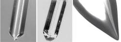
Lenses produced on the ends of optical fibers, for instance, have a host of uses based around their ability to improve and control the coupling of light into and out of the fiber (see Fig. 1). These lenses are used extensively in fiberoptic telecommunications, but also provide efficient and flexible optical probes in other applications like biomedical gel scanning, silicon-wafer fluorescence spectroscopy, and on-die VCSEL (vertical cavity laser) characterization.
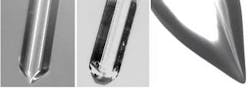
Quartz vacuum-chamber supports provide mechanical support for components and samples within a range of treatment chambers, including ion-implantation, x-ray crystallography, and x-ray photoelectron spectroscopy. These supports must be vacuum-compatible with very low thermal conductivity, and the material must be capable of withstanding the considerable temperature difference between the sample under test and the enclosure (see Fig. 2). Laser machining of the part allows the mechanical strength to be achieved while minimizing physical contact with the sample being held, thereby further reducing heat transfer as well as minimizing contamination of the sample or the measurement data.
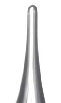
The end of a quartz lamp cut by laser is clean, smooth, and has gently rounded robust corners with no need for post-process flaming (see Fig. 3). Moreover, these parts are directly cut to precise length tolerances, eliminating the need for grinding, polishing, and cleaning steps to achieve tolerance. Laser cutting also allows the cut ends to be angled or chamfered to facilitate subsequent assembly processes. The precise cutting and milling of features in capillaries and flat plates, and the ability to laser-weld these parts together is finding increasing use in "lab-on-chip" devices. In applications like this the laser-machining system is typically fully integrated with the production line and parts handling is automatic.
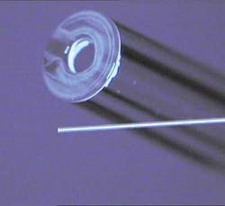
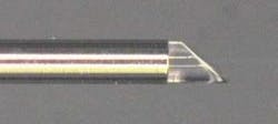
Both "lab-on-chip" and planar optoelectronic devices require the fiber end to be cut at angles of about 45° and rely on achieving total internal reflection off the inside of the angled face to couple light either in or out of the side of the fiber (see Fig. 4). The laser-cutting process can be applied to any requirement in which end-face angles from 0° to greater than 50° are required, and can also tailor the optical performance by using curved surfaces. The typical laser processing time for features such as this is less than one second.
The ability to reliably and efficiently process glass and quartz materials into new and complex geometries is opening new and exciting applications for what is a well-characterized and inexpensive material. Moreover, the capabilities offered by laser machining are bringing routine production to an area previously characterized by craftsman skill.
MIKE OSBORNE is technical director at OpTek Systems, Abingdon, England; e-mail: [email protected].