OTDR systems characterize faults in optical fiber
Bonnie C. Baker
The increasing use of optical fibers for worldwide communications is spurring development of optical time-domain reflectometer (OTDR) applications. Evolving telecommunications system requirements together with improved electrical components mean fiberoptic cable lengths between repeaters are increasing, making breaks or imperfections in the optical fiber more difficult to find. Nonetheless, technicians and field engineers must find ways to test and maintain these fiberoptic lines. Hence OTDRs, once found only in specialized applications, are proving useful for more-generic fiberoptic maintenance applications.
The OTDR technique
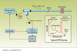
Fiber faults and defects are located by generating a short pulse with the OTDR driver circuit to the diode laser (see Fig. 1). This pulse transmits an optical signal down the fiber to the point of a fault or defect. The light is then reflected by the imperfection back to its origin. A critical part of the OTDR is the interface between the electronics and the fiber. Signals are transmitted through the fiber at the speed of light, thus high-speed transconductance amplifiers are crucial elements in the sensing portion of the OTDR circuit.
Two phenomena are monitored in order to retrieve the information needed to identify fiber defects. First is Fresnel reflections, caused by the difference between refractive indices of two mediums. A Fresnel reflection could occur, for example, if there were a connector, mechanical splice, or fault in the optical fiber. If air separates two fibers, the power of the reflected light is typically 4% of the total power. This type of break is shown in the OTDR application as a pulse or spike in the backscattered signal of a typical CRT display (see “Interpreting an OTDR display”).
The second phenomenon monitored with OTDR testers is Rayleigh backscattered light. If a pulse travels through a fiber and hits an imperfection, the light will scatter. The level and slope of the backscatter region in the response curve can be measured to determine the location of a fault or the onset of a potential break.
Receiver circuit design
Optical time domain reflectometers must measure imperfections accurately over fairly long distances (up to 20 km), starting from the point on the fiber where the diode laser is located. Such versatile measurement capability places difficult requirements on the optical receiver circuitry (see Fig. 2). In this circuit the photodiode used to receive light reflections from the fiber is reverse-biased to reduce the diode capacitance. The photodiode output response is current and is converted to a voltage using an operational amplifier with high input impedance or low input bias current and a resistor as the feedback element around the amplifier. The resulting voltage output of the amplifier is conditioned by the signal-processing unit in the OTDR test block.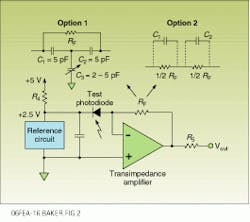
The dynamic range of an OTDR signal is expanded with a high-precision transimpedance amplifier. The operational amplifier in this circuit should have low input bias current, low noise, and a wide bandwidth in order to meet the dynamic-range requirements. Additionally, reducing the overload recovery time of the optical receiver circuitry will improve resolution in the dead zone. This reduction can be accomplished by inserting an optical switch in the front end of the receiver. The switch prevents the light and the Fresnel reflection—generated when the diode-laser pulse is transmitted—from entering the receiver. Another approach is to use an operational amplifier that can recover quickly from an overdrive condition into its linear output region; this approach can be followed exclusively or in conjunction with the optical switch.
Transimpedance amplifiers are used in a variety of applications, ranging from precision measurement devices such as medical blood-analyzer circuits to high-speed designs such as fiberoptic receiver circuits. Precision circuits typically require amplifiers with low offset voltage, low input bias current, low input capacitance, low voltage noise, and low current noise. With high-speed designs, the amplifier`s slew rate, bandwidth, input capacitance, and the parasitic capacitance of the circuit are critical to achieving high-speed performance. The combination of precision and speed is challenging because of the limited selection of amplifiers available.
In the circuit shown in Fig. 2, the photodiode can be configured with or without a bias voltage. If speed and response time are important, the photodiode is typically configured with a reverse bias voltage to lower the junction capacitance. Voltage feedback amplifiers, as opposed to current feedback amplifiers, are a natural choice for transimpedance amplifier circuits. Typically, the photodiode is selected for its responsivity and physical dimensions. The gain is then adjusted by changing the feedback resistor, RF.
If input bias currents in the microamp range are too large or cause unacceptable offset errors, alternative circuits can be implemented. One topology would use discrete field-effect transistors (FETs) and a high-speed amplifier. Another would use a voltage feedback amplifier with a FET input, such as the Burr-Brown OPA655. This FET-input voltage feedback amplifier is in a class of its own, with a typical unity gain bandwidth of 400 MHz and input bias currents of 5 pA.
Whatever the final transimpedance amplifier solution, it should be sufficiently stable with a bandwidth wide enough to accommodate the speed of the input signal. The variables in this design problem are the photodiode, the operational amplifier, and the feedback network of the operational amplifier. Optimum bandwidth is difficult to achieve for high-speed applications because of the pole set by the feedback capacitor, CF, and the feedback resistor, RF. In order to increase the pole frequency of the feedback loop and increase the bandwidth response, CF must be designed at a low value, typically less than 2 pF. This uncommonly low value can be achieved with either of the two circuit options shown in Fig. 1. In option 1, the T-network uses two 5-pF capacitors and a trim capacitor to design the low value capacitor. The effective capacitance of this circuit is equal to (C1C2) / (C1+C2+C3). If an inexpensive sub-picofarad capacitance is required, option 2 is recommended.
With this series-resistor topology, the resistance adds and the discrete capacitances divide. The effective resistance of this network is 1/2 RF + 1/2 RF = RF and the effective capacitance of this circuit is C1C2/(C1+C2). This option can be implemented with one capacitor, such as C1, and no discrete capacitor for C2. Then C2 would be replaced by the parasitic capacitance of the resistor and printed circuit board, which could easily be as low as 0.2 pF using standard RN55D resistors and careful layout techniques. As a result, the circuit can be designed with feedback capacitance lower than the capacitance achievable with a single resistor and no discrete capacitor. A reference circuit, such as the Burr-Brown REF1004-2.5 which is a 2.5-V reference, is added to provide a stable reverse bias voltage across the photodiode. In this circuit, the OPA655 can also be used as the cable driver, using R5 for the 50-W termination resistor.
The small-signal bandwidth of this transimpedance amplifier is shown in Fig. 3. In both cases the feedback capacitor, RF, is 2 × 274 kW. In trace #1 of Fig. 3, left, the photodiode was reverse-biased with 2.5 V, causing a parasitic capacitance across the photodiode of 27 pF. The -3-dB bandwidth of this trace is measured at 1.927315 MHz. The effective capacitance in the feedback loop is ~0.151 pF. Notice the small amount of gain peaking of approximately 1 dB. In trace #2, the photodiode was reverse biased with 5 V, causing a parasitic capacitance across the photodiode of 20 pF. The signal bandwidth is slightly increased to 2 MHz. To achieve this performance, care should be taken to remove the ground plane from areas where the inverting input and feedback resistors are located.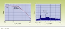
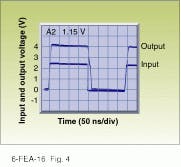
As measurement of optical fiber characteristics becomes an increasingly critical installation and maintenance issue, OTDR equipment offers a relatively easy method for technicians and field engineers to find faults in fibers and maintain fiberoptic communication lines. The OTDR system requires a sensitive test interface implemented with a transimpedance amplifier, such as the OPA655, that offers low input bias currents, high bandwidth, and fast overvoltage recovery time with no long-term tail that would mask the backscatter (see Fig. 4). Such critical design issues make implementation of increasingly accurate OTDR systems a continued challenge for the analog circuit designer.