Optical interconnects with nanolaser arrays?

In today’s Information Age, optical integrated devices are garnering attention as an alternative to electronic integrated devices, which are struggling to keep pace with the constant flood of data.
High-density integration of small light sources and their efficient driving and control are key components of optical technology, but as the density of laser arrays increases (or the spacing between lasers becomes narrower), placing and driving electrode arrays within a very tiny space is rapidly reaching its limits.
Fortunately, a team of researchers led by Myung-Ki Kim at Korea University’s Light Engineering Laboratory has shown that densely integrated nanolaser arrays can be fully driven and programmed with light through a single optical waveguide port—and it looks extremely promising for optical integrated circuits and interconnects.
Driving nanolaser arrays via light/optical waveguide port
To supply current to the laser array, a pair of electrodes must be introduced for each individual laser, which incurs significant on-chip space and energy consumption and processing delay.
This critical limitation can be maneuvered around by replacing the electrical drive with an optical drive. Unlike electrons, light is a wave that can form free spatial interference patterns. If the spatial interference patterns of light are used as a driving source of the laser array, an ultrahigh-density laser array source can be achieved.
“We’ve experimentally demonstrated that a three-dimensional nanolaser array densely printed onto an optical microfiber can be driven and programmed by switchable modal interference of the pump beam through the same fiber,” says Kim, an associate professor.
The team printed multiple photonic crystal nanolasers with a laser spacing of 18 µm on a 2-µm-diameter optical microfiber in 2D and 3D fashion using transfer-printing techniques and controlled multiple guided modes of the pump beam to selectively drive the laser array (see Fig. 1).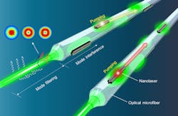
“We programmed the interference pattern by adjusting the pump beam’s polarization and pulse width,” says Kim, and “observed that the printed nanolaser array could be fully controlled by the pump beam’s modal interference. Then we confirmed our observations with numerical calculations.”
Through this work, the team was able to reduce the overall dimensions of the laser array compared to conventional electrically driven laser arrays by eliminating large and complex electrodes, and fundamentally minimized heat generation and processing delays caused by electrodes.
A need for speed/optical integrated circuits
Semiconductor electronics are helping to meet the demand for processing massive quantities of data, thanks to advances in complementary metal-oxide semiconductor processes to enable the very-large-scale integration of transistors.
“As semiconductor chips become more compact, the fabrication processes become more complex and expensive, and technology is approaching the physical limits due to quantum tunneling—inevitably causing energy dissipation and limiting the bandwidth for information processing,” says Kim.
So optical integrated circuits are emerging as an alternative—replacing electrons within circuits with light. “It’s an integrated system that detects, generates, transmits, and processes information through light on a microchip. Electronic transmission/interconnects is a major contributor that consumes a lot of energy and seriously slows down processing speed. We’re focusing our research on optical interconnects to replace these electrical interconnects with light.”
The use of optical waveguides instead of copper wires inside the chip enables much higher bandwidths while generating less heat in the interconnects. The challenge is that as the size of integrated circuits pushes into the nanometer regime, chip-scale optical components (lasers) must be highly integrated, and future solutions must be provided to drive and control them efficiently.
“Our work provides a new solution for higher-density laser arrays, which is essential for the development of optical interconnects, and can be a key technology for future development of optical integrated circuits,” says Kim.
The key to validating the team’s work was 3D alignment of III-V nanolasers on the surface of an optical waveguide, based on the interference pattern of the pump beam (see Fig. 2).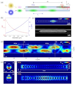
“To achieve this, we developed a high-resolution micro-transfer printing technique,” explains Kim. “Nanolasers freestanding on a III-V wafer were prefabricated, and the nanolasers were detached using a high-resolution confocal microscope and a micron-sized polydimethylsiloxane (PDMS) stamp. Then, the detached lasers were precisely printed in 3D on a 2-µm-diameter optical microfiber using a 360° continuous-rotation stage and a high-precision nanopositioning stage.”
A role for nanolaser arrays in optical interconnects
Optical interconnects are a key technology that has the potential to fundamentally solve many data center problems—including latencies/speed—and elevate their performance.
“Our information-centric world requires constant scaling of bandwidth, coupled with the demand for better utilization of hard-working data centers,” says Kim. “To accommodate this, data center architectures must continuously evolve, and new technologies must constantly be developed.”
Development of optical interconnects equipped with high-density nanolasers may “dramatically expand the data center’s information processing and allow us to stream ultrahigh-definition movies, scale interactive online encounters and games, accelerate the expansion of the Internet of Things, and provide the fast connectivity needed for big data analytics,” Kim points out.
The team’s work demonstrates all-optical driving and programming of densely integrated nanolaser arrays is indeed possible via modal interference of a pump beam. This technology can also be applied to chip-based silicon photonics systems, which may play a key role in the development of chip-to-chip or on-chip optical interconnects.
To apply their all-optical laser driving and programming technology to silicon photonics, it’ll be necessary to prove how independently the modes of a silicon waveguide can be controlled. “If this technology is developed, it’ll be a huge leap forward in the advancement of on-chip optical interconnects and optical integrated circuits,” Kim adds.
FURTHER READING
D. I. Song et al., Optica, 9, 12, 1424–1432 (2022); https://doi.org/10.1364/optica.471715.
About the Author

Sally Cole Johnson
Editor in Chief
Sally Cole Johnson is Laser Focus World’s editor in chief, and she has more than 25 years’ experience as a science and technology journalist. She specializes in physics and semiconductors, and wrote for the American Institute of Physics for more than 15 years, and also covered theoretical physics and neuroscience for the Kavli Foundation, and complexity for the Santa Fe Institute. Johnson has also written extensively about military embedded systems, high-performance computing, software-defined networks, and infosec.
When she isn’t writing about optics, photonics, or quantum advances, you can find her outside in northern NH in the garden with birds landing in her hand or heading for the mountains with her bike, skis, or crampons and ice axe.