Beneq: Enabling new optical coating solutions with ALD

2001 was a historically tough year for the optical communications industry. Companies across the globe were pivoting to reinvent themselves amidst the telecom bubble burst. It was a volatile time—and not the best for a Finnish engineer to be entering the space—but that didn’t stop Sami Sneck.
Graduating from what was then called the Helsinki University of Technology (today known as Aalto University) with a degree in chemical engineering, Sneck was seeking a job as the industry reeled. When he thinks back on that time, he calls out a particular mandatory class—one he dismissed as unnecessary when taking it—as a key piece of his professional trajectory: CAD drawings for equipment manufacturing. He remembers questioning why he would need that course and feeling frustrated with its requirements, but ultimately, it prepared him for a path that has been the foundation of his career. As Sneck readily points out, it just goes to show that it’s impossible to predict where things will go.
An entrepreneur by opportunity
Foreshadowing aside, Sneck put his skills to clever use in the industrial equipment manufacturing space, working for a company called Nextrom as a product manager. Then, in 2005, just a few years into his tenure, Nextrom refocused its priorities and decided that helping companies test, pilot, and manufacture new industrial products no longer fit with its larger-scale mission. Fortunately, three Nextrom employees saw the potential of that approach and decided to spin off and form Beneq.
When Beneq launched, it was a scrappy startup with approximately 10 employees. Work began to center on ways to shape the company vision and develop products into viable market solutions, and with that intensity of focus, Beneq began to build a niche expertise in atomic layer deposition (ALD). Little did Sneck know that this new role would be what skyrocketed his career.
The home of ALD
ALD technology was invented in Finland, where Beneq is headquartered, in the 1970s. Still today, Beneq feels it’s the natural home for ALD technology, with its roots remaining firmly planted in Espoo, Finland.
With that local foundation, it makes sense that the first members of the Beneq team each had a preexisting background in ALD. Couple that knowledge with expertise in manufacturing optical fiber preforms, and it was no time before the team was exploring how their ALD equipment could be applied to manufacturing optical fiber solutions.
Strategic R&D for ALD
While the optical communications market was beginning to rebound in 2005, it was nowhere near its pre-bubble steadiness and ALD was still a somewhat nascent technology. So, the Beneq team knew they needed to widen their net for potential opportunities. With that in mind, they directed their focus on a solution that allowed engineers to experiment with the technology.
According to Sneck, in the early days of Beneq, the team created an R&D machine so people could conduct research and explore ways that ALD could benefit their needs. Leadership placed a primary emphasis on research equipment and building relationships via university studies. The strategy centered on leveraging the research equipment side of the business to bolster the industrial business and help raise Beneq’s profile within the industry. In addition, by staying close to the trends emerging in the research world, the company could position and prepare for when those applications rose to market scalability.
A global player
Fortunately, Beneq was also a global entity from the beginning. From the Nextrom days, connections and customers existed outside its home base of Finland. So as the company geared up, it was able to lean into and grow its business overseas. This led to having new local offices to open up new possibilities in new industries. From that vantage point, they explored applications relating to photovoltaics and display technology.
Sneck also indicated that markets such as China are wonderful places to learn. With teams there exploring many different emerging technologies, it gave Beneq a chance to take in how those developments could factor into the company’s next steps.
Growing potential
To that end, Beneq still seeks ways to expand its presence in new spaces. For instance, Beneq’s leadership recognizes emerging markets that are benefiting from the power of semiconductor technology and advanced sensors—and trust ALD can play a role in their fabrication. The company’s coating technology rivals current solutions and offers efficiencies and impressive performance.
In addition, Sneck expects new potential to emerge. With advanced manufacturing needs for silicon photonics, micro-LEDs, green technologies, and so much more, ALD may just step in as a solution—if it can match necessary speed and performance. ALD faces challenges in these areas—it can be slow from the deposition rate point of view—but Sneck is quick to emphasize that the thickness of the deposit fields can determine the best fits. Often, they are relatively thin, less than 100 nm, but in some cases, like for optical coatings, they can be several microns thick and those take more time. Fortunately, Beneq has developed a system to address these needs and sees it as a potential option as the industry evolves.
Scaling up
As the company continues to explore new avenues for growth, they are also looking to be able to expand to a larger scale. Having larger equipment will create opportunities for 3D objects and other market demands. According to Sneck, that focus is the biggest driver for them right now—to learn how to fabricate large parts that are being deployed in semiconductor manufacturing equipment: chemical vapor deposition (CVD), plasma activated chemical vapor deposition (PCVD), ALD equipment, some types of LEDs with built-in reflectors, and others.
Today, the camera lenses in modern phones are already coated with ALD for superior antireflective properties, so Sneck sees the potential for it to be more widely leveraged in high-curvature lenses, emerging camera lenses, and anything needing optical domes that function like a camera or detector inside. In addition to antireflective coating solutions, another huge area of opportunity comes in the form of augmented reality and its corresponding lenses. More consumer electronics may see the introduction of this coating as the space continues to evolve.
Sneck also recognizes a wide-reaching potential in industries as diverse as security, autonomous vehicles, free-form optics, nanoprints and 3D prints, and so much more. Any kind of complex shape is good for ALD because it’s difficult for other coatings to align efficiently and effectively.
Building for the future
With that potential in mind, there’s so much more to come.
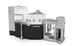
Today, Beneq employs approximately 150 people and is one leader in the market with innovative solutions for advanced R&D (TFS 200, TFS 500), flexible high-volume manufacturing (BENEQ Transform), ultrafast high-precision spatial ALD coatings (C2R), roll-to-roll thin film coating of continuous webs (WCS 600), and specialized batch production for thicker film stacks (P400, P800).
They also have become the the engine of ALD, propelling the solution’s potential and performance. Sneck firmly believes that as the industry catches on, more advanced device and optical coating designs will be enabled with ALD. In fact, in five years, he expects more companies and people will adopt it in optics and photonics, and it will drive innovation—new ideas that they have yet to imagine—making ALD a prominent optical coating technique.
For a company that has a history of being the first in the world to try a new concept, it doesn’t seem unlikely that novel use cases for ALD, from new material structures to completely new innovative products, will materialize. Though, given that the company’s name literally translates from Latin as “good equipment,” that should come as no surprise.
ACKNOWLEDGMENT
BENEQ Transform is a registered trademark of Beneq.
About the Author
Jose Pozo
Chief Technology Officer, Optica
Jose Pozo joined Optica in March 2022, and has spent more than 25 years working in photonics. He earned a PhD in quantum physics from the University of Bristol (U.K.), and an M.Sc. and B.Eng. in telecom engineering from UPNA, Spain / VUB (Belgium). Prior to joining the European Photonics Industry Consortium (EPIC) in 2015 as CTO, Jose was a Senior Photonics Technology Consultant with PNO Consultants, with some of the main accounts such as CERN, Thales, and TE Connectivity. He has worked at TNO, The Netherlands Organization for Applied Scientific Research, and as a postdoctoral researcher at the Eindhoven University of Technology in the Netherlands, where he contributed to the early development of EFFECT Photonics.