Atmosphere Furnaces in Semiconductor Fabrication: Annealing, Oxidation, and Diffusion
Semiconductor device fabrication in the United States is defined by controlled thermal budgets, ultra-high cleanliness, and atomic-scale defect sensitivity. At the heart of these heat-driven processes sits the atmosphere furnace—a sealed thermal system engineered to process wafers under optimized gas environments. From dopant activation to oxide interface formation and solid-state drive-in diffusion, controlled atmosphere furnace platforms deliver precise conditions required for repeatable and publication-grade research.
Unlike open heating systems, which expose surfaces to uncontrolled oxygen and moisture, inert atmosphere furnace chambers manage ambient isolation with nitrogen, argon, hydrogen, or hybrid vacuum modes. In USA university nanofabrication labs and semiconductor research cleanrooms, this capability is vital for ensuring doping uniformity, gate oxide integrity, and diffusion junction depth control.
Understanding Atmosphere Furnace Technology
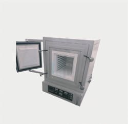
An atmosphere furnace consists of:
● A sealed heating enclosure (box or muffle chamber)
● A reaction tube or sample vessel zone where wafers or materials sit
● Gas inlet/outlet manifolds for atmosphere creation
● Pressure-tunable environments (vacuum or low-pressure hybrid options)
In American semiconductor research, the most deployed variants include the horizontal and box-style atmosphere box furnace, along with muffle-type furnaces optimized to avoid heating-element contamination.
The term controlled atmosphere muffle furnace is especially relevant in U.S. semiconductor labs, where molecular insulation prevents furnace coil metal transfer to sample surfaces. Similarly, controlled atmosphere heat treatment furnace systems are adopted when researchers anneal, oxidize, or diffuse dopants into device substrates.
Orientation and Chamber Design: Atmosphere Furnace
USA laboratories typically deploy furnaces based on sample format and gas dynamics:
|
Furnace Type |
Design Format |
Wafer Processing Strength |
Research Usage |
|
Atmosphere Box Furnace |
Sealed box chamber |
Uniform batch processing |
Wafer annealing, oxide growth |
|
Controlled Atmosphere Muffle Furnace |
Coil-free or insulated chamber |
Eliminates metal contamination |
Oxidation, sensitive thermal analysis |
|
Vacuum Atmosphere Furnace |
Hybrid vacuum + gas ports |
Ultra-clean low-pressure processing |
Dopant diffusion science, thin oxides |
|
Inert Atmosphere Furnace |
N₂ / Ar / Argon dominant |
Oxide-free anneals |
Defect engineering |
|
Hydrogen Atmosphere Furnace |
Sealed H₂ heating |
Enables reduction + dopant mobility |
Surface and implant activation experiments |
|
Nitrogen Atmosphere Furnace |
Pure N₂ purge |
Stable oxidation carrier + safe heating |
Dominant rinse atmosphere |
|
Argon Atmosphere Furnace |
Noble inert gas |
Highest purity environment |
Wafer interface and diffusion kinetics |
Orientation (horizontal vs vertical) also influences gas physics. In nanofabs across the USA, horizontal tube chambers are often used for stable laminar gas diffusion across wafer surfaces, while vertical designs are reserved for powder or gravity-assisted melts—but wafer research overwhelmingly favors horizontal gas stability.
Why Atmosphere Furnaces Matter in Semiconductor Fabrication
In semiconductor fabrication and academic R&D workflows, furnace atmospheres directly affect:
● Crystal defect recombination
● Oxide nucleation rate
● Dopant mobility and electrical activation
● Junction diffusion depth
● Wafer interface stability
● Surface passivation quality
Even minor oxygen and moisture inconsistencies can result in:
● Dopant diffusion non-uniformity
● Electron trap density spikes
● Poor oxide tunneling layers
● Dislocation persistence post-implant
● Altered material phases
A controlled atmosphere heat treatment furnace allows researchers to eliminate these variables by supplying sealed, tunable gas environments for each experiment.
Key Process 1 — Annealing in Semiconductor Research
Annealing Goals
Annealing is a thermal activation cycle used to:
● Heal ion-implantation crystal damage
● Electrically activate dopants (e.g., B, P, As species)
● Reduce wafer stress after deposition or etching
● Improve grain structure in thin films
● Stabilize interfaces between substrate and passivation layers
In U.S. device labs, implant-activation anneals are routinely performed under:
● nitrogen atmosphere furnace or argon atmosphere furnace environments to suppress oxidation
● hydrogen atmosphere furnace modes for surface reduction prior to dopant drive-in
● vacuum atmosphere furnace hybrid systems for ultra-clean annealing without native oxide regrowth
|
Annealing Type |
Gas Atmosphere |
Why Used |
|
Post-implant activation |
Nitrogen / Argon |
Oxide-free dopant activation |
|
Thin film stress annealing |
Inert gas mix |
Prevents interface oxidation |
|
Surface reduction anneal |
Hydrogen (H₂) |
Cleans and mobilizes dopants |
|
Ultra clean anneal |
Vacuum + argon hybrid |
Minimal contamination |
Researchers frequently reference laboratory tube furnace thermo scientific platforms from Thermo Scientific for stable temperature and sealed gas reliability across long research cycles.
Key Process 2 — Oxidation Furnace Atmospheres
Oxidation in Semiconductor Fabs (USA)
Thermal oxidation forms silicon dioxide (SiO₂) or surface oxide films for:
● MOSFET gate dielectric layers
● Wafer isolation oxides
● Passivation films to reduce charge trap density
● Mask oxides for diffusion doping
● Field oxides to electrically isolate transistor regions
Oxidation may be “dry” or “wet” depending on oxide thickness goals, but USA academic labs strongly favor:
● controlled atmosphere muffle furnace chambers for contamination-safe oxide nucleation
● nitrogen atmosphere furnace carriers to control oxygen dilution
● vacuum atmosphere furnace modes when growing ultra-thin device oxides
These environments regulate oxidation rate and uniformity, ensuring defect-free tunneling and dielectric stability.
|
Oxide Layer Goal |
Furnace Mode |
Atmosphere Used |
|
Ultra thin gate oxides |
Vacuum hybrid |
Vacuum + dry O₂ |
|
Mask oxide for doping |
Controlled box / muffle |
N₂ + trace O₂ |
|
Isolation field oxide |
Box furnace |
Diluted or dry oxygen |
|
No metal contamination |
Muffle format |
Coil-insulated heating |
Key Process 3 — Dopant Diffusion and Drive-In Cycles
Diffusion Goals in USA Semiconductor Research
Dopant diffusion furnaces thermally migrate doping species into silicon or compound semiconductor substrates to form:
● pn-junctions
● Controlled CMOS junction depths
● Solid-state doped layers without epitaxy
● Boron/phosphorus thermal drive-in profiles for junction engineering
● Kinetic studies of dopant mobility
Dopant mobility behavior depends heavily on gas atmosphere:
|
Diffusion Focus |
Atmosphere |
Furnace Type |
|
Boron drive-in studies |
Nitrogen |
Nitrogen atmosphere furnace |
|
Phosphorus diffusion |
Argon |
Argon atmosphere furnace |
|
Enhanced dopant mobility |
H₂-inert mix |
Hydrogen atmosphere furnace |
|
Lowest contamination diffusion |
Vacuum + Ar hybrid |
Vacuum atmosphere furnace |
Because these furnaces are sealed during dopant migration, U.S. labs require strict purge sequencing:
- Initial moisture and oxygen evacuation or purging
- Inert gas stabilization phase (typically N₂ or Ar)
- Optional hydrogen reduction anneal
- Dopant drive-in thermal activation
- Cool-down under inert or vacuum protection
This sequence ensures that oxidation does not occur at unintended stages and dopants remain stable, electrically activated, and reproducible for characterization.
Furnace Atmosphere Switching for Multi-Process Wafer Research
USA research fabs routinely shift between multiple gases within the same furnace platform. Compatibility across:
● noble atmosphere gases → Argon, Helium
● inert gas suppressed oxidation anneals → Nitrogen, Argon
● reduction enhanced activation → Hydrogen
● ultra-controlled low pressure heat studies → vacuum-argon hybrid systems
This ability to manage environments is why atmosphere systems are referred to as atmosphere furnaces, inert furnaces, or controlled atmosphere heat treatment furnace modules in university research.
Safety Culture and Academic Responsibility in USA Nanofabs
While cost considerations are excluded in this version, USA academic labs emphasize safety based on:
● Gas exhaust routing safety
● Hydrogen and inert gas handling training
● Sealed chamber leak validation
● Reactor tube integrity inspection
● Avoiding over-temperature thresholds for quartz or alumina tubes
● Preventing gas accumulation and oxygen–hydrogen reactive mix hazards
|
Safety Standard |
Importance |
|
Tube inspection |
Prevent sample contamination |
|
Proper gas purging |
Prevent flash oxidation |
|
Shielding and PPE |
Prevent burn injuries |
|
Exhaust routing |
Avoid gas buildup |
Conclusion
Atmosphere furnaces remain fundamental to U.S. semiconductor fabrication research, offering sealed, gas-controlled environments for:
● Annealing (defect healing and dopant activation)
● Oxidation (contamination-safe oxide layer growth)
● Diffusion (precise dopant drive-in and pn-junction engineering)
Systems including horizontal furnace, atmosphere box furnace, vacuum atmosphere furnace, nitrogen atmosphere furnace, hydrogen atmosphere furnace, argon atmosphere furnace, inert atmosphere furnace, and partnerships through atmosphere furnace supplier networks drive scalable research across the United States.
Their ability to tune gas purity and pressure ensures reproducible wafer processing—supporting publications, PhD research, material characterization, and proof-of-concept device development.