Tucsen Presents Semiconductor Inspection Imaging Solutions at SEDEX 2026
The showcase covers three inspection regimes: high-speed front-end wafer and mask inspection, advanced packaging and automated optical inspection (AOI), and vacuum-based metrology using soft X-ray and extreme ultraviolet (EUV) light.
Across all three, equipment makers are being asked to reconcile the same set of demands at once — faster throughput, wider fields of view, and image stability that holds over long production runs. Tucsen’s response is not a single camera but a set of architectures, each built for a different point in the inspection workflow.
Matching Camera Architecture to the Inspection Stage
Tucsen’s semiconductor inspection solutions are organized around two inspection architectures: line scan and area scan.
For high-speed front end wafer and mask inspection, the Gemini TDI series uses multi-stage signal accumulation to raise sensitivity and signal-to-noise ratio while the stage is in continuous motion. The Gemini 8KTDI supports line rates up to 1 MHz at 8K resolution and moves data over a 100G CoF interface. The combination targets one specific problem: capturing low-contrast defects clearly without slowing the scan to buy exposure.
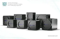
Where resolution and coverage matter more than raw line rate, the Libra series of large-format industrial cameras takes over. The recently introduced Libra 27105 pairs a 105 MP sony sensor with a 39.7 mm (2.5″) optical format and runs at 112 fps at full resolution. Imaging more area per frame cuts the amount of stitching a system has to perform, which matters for high-speed AOI, defect review, and inspection workflows built around AI -based defect classification.
Offering both architectures lets equipment makers and system integrators choose per stage. A wafer scanner and a packaging AOI station rarely place the same demands on a camera, and treating them as one problem usually forces a compromise somewhere in the image chain.
Imaging Where Visible Light and Ambient Pressure Are Not Options
Certain inspection and metrology processes fall outside the capabilities of standard visible light cameras. To address these applications, Tucsen has developed the Dhyana XF and XV series—vacuum-compatible sCMOS cameras designed specifically for the direct detection of soft X-ray and extreme ultraviolet (EUV) photons within high-vacuum chambers.
Both series utilize back illuminated sensors with high quantum efficiency and are designed to operate in vacuum environments down to 10⁻⁷ Pa. They are widely used in technical fields such as EUV inspection. Tucsen’s semiconductor product portfolio spans from conventional optical inspection to metrology and inspection tasks that must be performed in a vacuum or outside the visible light spectrum.
From Technology Development to Reliable Product Delivery
Behind the products sits Tucsen’s own engineering and manufacturing. Teams covering optics, electronics, mechanics, computing and software work from stated application requirements, with FPGA-based architectures, in-house SDK development, standardized interfaces and production-level integration handled internally.
Manufacturing runs across more than 10,000 square meters, including Class 100 and Class 1,000 cleanrooms and flexible production lines. Standardized processes in production, testing and quality control are what let a camera shipped this quarter behave like the one a customer qualified last year — a consideration that tends to outweigh any single datasheet number once a tool goes into a fab.

Tucsen also develops customized imaging solutions for inspection requirements that standard products do not cover, with the aim of shortening the path from evaluation to deployment.
A Platform Rather Than a Product Line
Tucsen’s approach in industrial semiconductor imaging has been to build the underlying technology platform first. In high-sensitivity imaging, that means continued work on low-noise design, quantum efficiency, thermal stability and broad spectral response — the properties that decide whether a weak signal is captured at all. In high-throughput imaging, it means large-format and high-speed camera platforms that raise inspection efficiency without letting image quality drift across a continuous run.
Combined with expertise in vacuum compatibility, deep cooling, ultra-low dark current control and extended spectral response, the portfolio spans front-end wafer scanning, advanced packaging, and specialized metrology.
Continuing the Conversation After SEDEX
Teams evaluating imaging for wafer inspection, advanced packaging or specialized metrology can reach Tucsen’s engineering group to discuss specific application requirements.
Product documentation and sample evaluation support are available on request. For more information, visit Tucsen’s semiconductor solutions page or contact the engineering team.
About Tucsen Photonics
Tucsen Photonics specializes in the research and development of scientific cameras for photon detection, providing imaging products and solutions for research microscopy, industrial inspection, and frontier exploration. The company advances imaging performance and application capabilities, supporting the adoption of photonic information technologies across scientific research and industrial applications.