Wooptix Installs First Phemet® Metrology System at CEA-Leti
Represents Wooptix’s first production deployment and establishes long-term collaboration with one of the world’s leading semiconductor R&D ecosystems
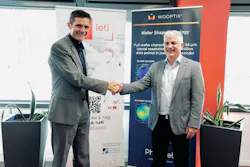
GRENOBLE, France and TENERIFE, Spain, June 29, 2026—Wooptix, an innovation leader in semiconductor wavefront phase imaging metrology, today announced the installation of its Phemet® system at CEA-Leti’s Grenoble technology research institute, marking a significant milestone in the company’s expansion into semiconductor metrology and process control. Installed on May 4, 2026, the system will support joint work on wafer-scale process signatures, nanotopography, and advanced packaging metrology in an industrial semiconductor cleanroom environment. The joint agreement was highlighted during CEA-Leti Innovation Days/LID World Summit, the institute’s flagship annual event that took place in June 23-25 in Grenoble.
“This installation marks a major milestone for Wooptix and a necessary step in our roadmap toward high-volume semiconductor manufacturing applications,” said José Manuel Ramos, CEO, Wooptix. “Our collaboration with CEA-Leti will allow us to validate Phemet® in a highly controlled semiconductor cleanroom environment and to build application evidence around real process-development challenges alongside some of the world’s leading players. The project strengthens our presence in Grenoble, a dynamic European semiconductor hub.”
The installation is the first deployment of Wooptix’s Phemet® production metrology tool. The collaboration will enable Wooptix to test and refine its technology directly in product-relevant processes while exploring new use cases within one of Europe’s most sophisticated R&D facilities.
“CEA-Leti is excited to evaluate the capabilities of the first fully automated Phemet® 300 mm platform—a significant milestone that will enable the deployment of a wide range of applications at industrial scale. Our collaboration with Wooptix opens new opportunities to tackle cutting-edge challenges in nanotopographic metrology,” said Viorel Balan, Collaboration Project Manager. “By leveraging the Phemet® platform, we aim to deepen our understanding of the processes, support research initiatives within European Union projects, and accelerate the development of next-generation advanced packaging technologies.”
Wooptix Phemet® Metrology System
Wooptix introduced its Phemet® metrology system in November 2025. It provides ultrafast and extremely accurate wafer shape and geometry measurements with sub-nanometer resolution. Phemet® addresses the growing demand for improved process control in high-volume manufacturing, especially as the industry continues to innovate with higher-performance, smaller and more complex devices with nanoscale feature sizes and novel integration approaches.