ON Semiconductor CMOS sensor produces 120 dB images

Feb. 12, 2018
The Hayabusa CMOS image sensor platform features a 3 µm backside-illuminated pixel design. 

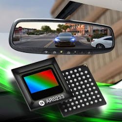
The Hayabusa CMOS image sensor platform features a 3 µm backside-illuminated pixel design that delivers a charge capacity of 100,000 electrons. It is designed for automotive imaging and includes simultaneous on-chip high dynamic range with LED flicker mitigation, plus real-time functional safety and automotive-grade qualification. It produces 120 dB images.

ON Semiconductor

Phoenix, AZ

www.onsemi.com

Sponsored Recommendations

Working with Optical Density

Feb. 26, 2025
Optical Density, or OD, is a convenient tool used to describe the transmission of light through a highly blocking optical filter.

Custom-Engineered Optical Solutions for Your Application

Feb. 26, 2025
Explore the newest and most widely used applications of Semrock optical filters.

Linear Stages & Rotary Stages for High Precision Automation & Motion Control

Feb. 13, 2025
Motorized Linear Translation Stages & Rotary Precision Positioning Stages for High Performance Automation & Motion Control | PI USA

Motion Controllers for Precision Positioning and Automation

Feb. 13, 2025
PI manufactures a range of precision motion controllers and drivers for positioning systems, including stepper motors, brushless motors, and servo motors.

Voice your opinion!

To join the conversation, and become an exclusive member of Laser Focus World, create an account today!