Nickel oxide, titanium dioxide, and gold nanoparticles form plasmonic visible-light solar cell
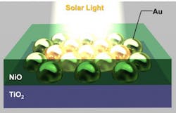
Scientists at Hokkaido University (Sapporo, Japan) and National Chiao Tung University (Hsinchu, Taiwan) have used atomic layer deposition to deposit a thin film of nickel oxide (NiO) onto a single crystal of titanium dioxide (TiO2); gold nanoparticles introduced between the two layers become plasmonic antennas that harvest visible light.1 Photocurrent generation was observed on the all-solid-state photoelectric conversion device. Being an inorganic solar cell, the device was found to be durable and stable.
The team tested the properties of these fabricated devices with and without annealing of the NiO. Annealing affected the properties of the device by changing the interfacial structure of the layers. For example, it increased the voltage available from the device but also increased the resistance within it. It also decreased the device's efficiency in converting light to electricity.
The results suggest that the structural changes caused by annealing prevent the layer of gold nanoparticles from injecting electrons into the titanium dioxide layer. The fabrication process is inexpensive and can be scaled up easily, but the resultant device's properties are still insufficient for practical use and its efficiency in converting light to energy needs to be improved. Further research is needed to understand the roles of each layer in conducting energy to improve the device's efficiency.
REFERENCE
1. Keisuke Nakamura et al., Journal of Physical Chemistry Letters (2016); doi: 10.1021/acs.jpclett.6b00291.
About the Author

John Wallace
Senior Technical Editor (1998-2022)
John Wallace was with Laser Focus World for nearly 25 years, retiring in late June 2022. He obtained a bachelor's degree in mechanical engineering and physics at Rutgers University and a master's in optical engineering at the University of Rochester. Before becoming an editor, John worked as an engineer at RCA, Exxon, Eastman Kodak, and GCA Corporation.