Three semiconducting sulfides in one nanocrystal extend solar-cell range to the UV and IR
Common solar cells made of crystalline silicon can only access roughly half of the total sunlight spectrum for conversion of light energy into electricity. Searching for more-effective photovoltaic (PV) materials, scientists at the University of Science and Technology of China (Hefei, China) have combined three types of semiconducting sulfide crystal into one nanocrystal to form a ternary nanostructured photovoltaic system that absorbs irradiation from the UV to near-IR regions.1 The nanorods effectively convert the full-spectrum light energy into electric current.
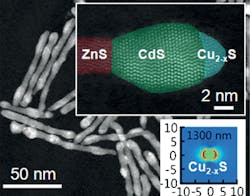
ZnS, CdS, and Cu2−xS all in oneThe PV material most commonly used today is crystalline silicon, which absorbs sunlight effectively only in the visible region. Other semiconducting materials cover slightly different regions of the solar spectrum, but the most-efficient PV materials would be clearly those that include a wider spectral region. The new nanostructured system made of three sulfide crystals is a hybrid material of zinc, cadmium, and copper sulfides that absorbs from UV to near-IR; each nanorod has a segmented node-sheath structure that provides the ideal energy-band alignment for an effective accumulation of charge carriers.
The zinc sulfide (ZnS) base rod provides the UV absorption, while the cadmium sulfide (CdS) addition covers the visible light region. For IR absorption, the scientists chose copper sulfide nanocrystals with copper deficiencies (Cu2−xS), as this material is known to feature a special type of absorption in the near-infrared region called surface plasmon resonance. "These heteronanorods absorb across nearly the full spectrum of solar energy," the scientists report.
To test the functionality of the nanorods, the scientists measured their performance in a photoelectrochemical water-splitting cell. Upon full-spectrum illumination, the photocurrent response was pronounced. One of the crucial achievements of this work, however, was the correct adjusting of the sensitive heterojunctions that connect the different semiconducting structures to align the energy gaps of the semiconducting materials.
"Such a staggered alignment enables the separation of the photogenerated electrons and holes in the ternary hybrid nanostructure," say the authors. Although further experiments need to be performed, this ternary semiconducting system is a step toward a new generation of efficient wide-spectrum solar cells.
Source: http://onlinelibrary.wiley.com/journal/10.1002/%28ISSN%291521-3773/homepage/press/201613press.html
REFERENCE:
1. Tao-Tao Zhuang et al., Angewandte Chemie (2016); doi: 10.1002/anie.201601865
About the Author

John Wallace
Senior Technical Editor (1998-2022)
John Wallace was with Laser Focus World for nearly 25 years, retiring in late June 2022. He obtained a bachelor's degree in mechanical engineering and physics at Rutgers University and a master's in optical engineering at the University of Rochester. Before becoming an editor, John worked as an engineer at RCA, Exxon, Eastman Kodak, and GCA Corporation.