CMOS detectors nip at the heels of CCD devices

After decades of research and development, complementary metal oxide semiconductor (CMOS) detectors may be on the verge of replacing the ubiquitous charge-coupled device (CCD) in a variety of applications, and not necessarily just in imaging. The CMOS devices, which reside on the same type of chips used for microprocessors, are benefiting from the massive investment made in microprocessor manufacturing technology over the past years. As a result, they are lower in cost than CCDs, consume less power, and, because of the many transistors built into them, offer higher versatility.
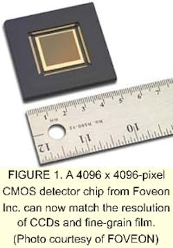
Until this past year, though, their resolution kept CMOS devices from competing head-on with CCDs—but no longer. Foveon Inc. (Santa Clara, CA) has released a 4096 × 4096-pixel CMOS detector chip capable of matching the resolution of both CCDs and fine-grain film (see Fig. 1). Such high-resolution CMOS devices as this may have the power to dramatically chip away at the market held by CCDs.
Decades of R&D payoff
Detector researchers and end users have long recognized that CCDs have significant drawbacks despite their usefulness. These detectors operate by transferring charge, bucket-brigade style, from each pixel to the edge of an array. Since charge is transferred many times, they require extremely high accuracy. They are thus vulnerable to relatively low levels of radiation, which is a disadvantage for space applications. In addition, their auxiliary circuits are relatively power hungry relative to the timing and voltage shifts needed to transfer the charges; they are also limiting factors in further CCD miniaturization efforts. Unlike CMOS sensors, CCDs also require a specialized production process.
As early as 1968, scientists were proposing CMOS detectors, then called active-pixel sensors, as a way of overcoming these drawbacks. In these devices, individual photodetectors (similar to a single CCD pixel) are integrated with individual transistors or groups of transistors so the array can be read across wires much like random access memory. Unlike CCDs, the detectors also can integrate all functions from detection to amplification, and timing on one chip, and their power draw is orders of magnitude smaller. In addition, because a defect will only affect a single pixel, instead of a whole line of pixels, CMOS devices are relatively radiation hard. Their low-cost high-volume manufacturability method only adds to their competitiveness.
The high-resolution chip developed by Foveon in cooperation with National Semiconductor Corp. (Santa Clara, CA), for example, uses the latest 0.18-µm line-width processing. With 70 million transistors, five for each pixel, the chip has 2.5 times as many transistors as Intel Pentium II microprocessors. It measures only 22 mm on a side, which facilitates its integration into small cameras, yet offers resolution previously only attainable with larger cameras.
Around the same time Foveon introduced its chip, Eastman Kodak (Rochester, NY) announced plans to market a 4096 × 4096-pixel CCD, so regardless of any advantages one detector type has over the other, they are now matched in resolution, and both meet or exceed the resolution of most photographic film. Since the human eye can resolve details approaching one arc min (1/3000 of a radian) across, photographs with 4000 pixels across are perceived as being grain-free, even at large sizes.
The Foveon chip, with a brightness-to-darkest ratio near 1000, also matches CCDs in dynamic range. This is equivalent to film with an ISO rating of 100, in addition to matching the new Eastman Kodak CCD in sensitivity (although specialized CCDs can still have a sensitivity advantage). End users should expect to see the new CMOS chips in high-end cameras sometime early next year and can already find earlier versions of the chip with half the resolution in Hasselbad cameras.
Smarter chips for smarter images
The CMOS chips have another advantage because of their ability to use on-chip computing power to become more versatile imagers, especially in ways related to dynamic range. Although the human eye can detect light over a dynamic range approaching a factor of 1010, even the typical CCD has a range factor close to just 1000, which can lead to blooming of bright areas and complete lack of detail in dark areas of a typical scene.
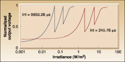
In their efforts to enhance the dynamic range of CMOS detectors, a German research team supported by auto manufacturer BMW has developed a 256 × 256 CMOS chip with a dynamic range factor approaching a million for use in an automotive scanning system or "driver's assistant." Each pixel, which has its own gain and shutter speed (or integration time), is sampled repeatedly during the overall interval of a single frame or exposure (with 50 frames/s recorded). The image controller circuit selects the longest exposure time per pixel that will not saturate it and records that time as a 2-bit code. Integration times from 20 µs to 5 ms are thus possible.1
As an individual pixel collects light and approaches saturation, the system's circuits can adjust gain by reducing it to a lower level (see Fig. 2). Both integration time data and this gain information, also recorded as a 2-bit code per pixel, are combined with a 14-bit pixel output signal to form a 20-bit measurement of light intensity. This method is reportedly accurate to one part in a thousand.On-chip computation also has other potential applications, including target tracking in industrial, surveillance, and navigational devices. Researchers have even put considerable effort into mimicking the biological tracking capabilities of the human eye.
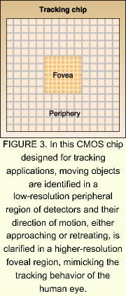
A team of researchers from Johns Hopkins University (Baltimore, MD), the University of Pennsylvania (Philadelphia, PA), and Corticon Inc. (Philadelphia, PA) has developed a CMOS chip for tracking that has a high-resolution foveal region and a lower-resolution peripheral region (see Fig. 3).2 While the research prototype uses fewer than 400 pixels, it reportedly has "respectable" performance levels. In both the fovea, a 9 × 9-pixel dense array, and the periphery, a sparser 19 × 17-pixel array, gain control allows a dynamic range factor approaching a million with a logarithmic response in low light and a linear relationship in bright light. Edge-detection circuits highlight areas of rapid change in contrast, thus defining potential targets to be tracked.In the periphery, the device calculates the centroid of each object for each frame. Once the edge detectors define the object, the centroid location is determined by an intensity-weighted average of all pixels within the edges. To speed computation, the system uses analog circuit elements to obtain the averages of the intensities. In a complete tracking system, the signal from the periphery can be used to move the image of an object into the fovea for more-precise tracking.
In the foveal region, additional circuits measure the direction of motion of individual edges. In a process inspired by the visual system of a fly, the motion-detection circuit correlates the disappearance of an edge in one pixel with the appearance of an edge in one of its neighbors. Each pixel thus sends out its own signal detecting the direction of motion of the object, with the signal to the tracking motor being the sum of the individual signals. If an object is approaching, but also moving in a given direction, that direction is the one conveyed to the tracking motor.
Despite its relatively low resolution, the scientists successfully used the chip to track objects moving as fast as 10,000 pixels/s and to guide automated vehicles around obstacles. Issues still to be addressed with the chip include improving range and enhancing the device's ability to distinguish targets in a "noisy" environment.
Speeding up optical communications
Another application area where CMOS sensors may someday have an advantage over CCDs is optical communications. In the past, the use of CMOS sensors in such systems was limited by detector response time, which in turn limited the rate at which information can be received. In a conventional CMOS detector, carriers are generated over a depth of 15 µm, the absorption length of 860-nm light. The charge carriers generated at shallow levels are detected immediately, but others generated at greater depths in the substrate diffuse slowly to reach the p-n junction microseconds later. This time lapse blurs out the pulses because current continues to rise long after a pulse has started and continues to decline after it has ended, creating what is called low-frequency gain.
In an attempt to eliminate this gain and allow higher bit rates, researchers at the University of Brussels (Brussels, Belgium) have designed a spatially modulated light detector that cancels out the low frequency gain, while maintaining high frequency gain.3, 4 The device comprises a row of rectangular p-n junctions, every other one of which is covered by light-blocking material. The masked detectors combine to form the deferred detector, the unmasked ones are the immediate detectors.
When a light pulse arrives, the unmasked detectors will immediately detect shallower carriers. The masked and unmasked detectors will spot those diffusing from greater depths at about the same time. Subtracting the response of the deferred detectors from that of the immediate detectors thus eliminates the effect of the slower carriers. Using this technique, the Brussels team has fabricated a 100-channel array on a 1-mm2 chip that has a total capacity of 20 Gbit/s.
With such advances, prospects for rapid expansion of CMOS technology are getting brighter.
REFERENCES
- M. Schanz et al., IEEE J. of Solid State Circuits 35, 932 (July 2000).
- R. Etienne-Cummings et al., IEEE Trans. On Circuits & Systems II 47, 504 (June 2000).
- M. Kuijk et al., SPIE Proc. 3952, 98 (January 2000).
- C. Rooman et al., IEEE J. of Solid State Circuits 35, 953 (July 2000).
About the Author
Eric J. Lerner
Contributing Editor, Laser Focus World
Eric J. Lerner is a contributing editor for Laser Focus World.

