Researchers improve 10 Gbit/s photoreceiver

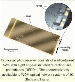
Optical network systems based on wavelength-division multiplexing (WDM) require photoreceivers that can efficiently convert optical signals into electrical signals. Making use of recently developed technologies, researchers at NTT Photonics Laboratories (Ibaraki-ken, Japan) have fabricated and tested a hybrid multiwavelength photoreceiver with eight channels that shows promise for compactness as well as high speed in WDM network systems. Combining planar lightwave circuit (PLC) technology with hybrid integration of photodiodes on arrayed waveguides (AWGs), the photoreceiver consists of refracting-facet photodiodes (RFPDs) incorporated on a silica-based AWG demultiplexer (see figure).
The photoreceiver consists of eight edge-illuminated RFPDs on a 1 x 8 AWG with channel spacing of 525 GHz. To simplify the process for fabricating a PLC platform on an AWG, Takaharu Ohyama and colleagues introduced a novel assembly region without a silica-on-terraced silicon (STS) structure. In conventional PLC platforms, the STS structure provides a precise height reference to align optoelectronic devices with the waveguide core of the PLC. However, the team eliminated the STS fabrication process, which involves many steps such as chemical etching and mechanical polishing. The new assembly technique prescribes a precise thickness of undercladding to match the height of the silica-waveguide core of the PLC and the photosensitive facet of the RFPD. In addition, the unique photosensitive facet structure gives the RFPDs a wide alignment tolerance.
Parasitic capacitance between the RFPD electrodes and the silicon substrate are minimized to achieve 10 Gbit/s transmission by use of microsolder bumps for the electrical interconnections. The photodiodes are bonded at individual output ports of the AWG demultiplexer using gold-tin (Au-Sn) solder bumps with a diameter of 50 µm. To achieve multichip bonding on the same PLC platform, the researchers introduced an Au-Sn thin film solder technique, reflowing the hard bumps of all the chips at once in a nitrogen atmosphere. The multichip bonding technique facilitates high responsivity and high-speed operation.
The team measured the characteristics of the photoreceiver, and found the average peak responsivity for eight channels to be 0.6 A/W. This corresponds to the expected value considering the responsivity of the discrete RFPD and the insertion loss of the discrete AWG. The average 3 dB bandwidth of the responsivity was 353 GHz and the average crosstalk to neighboring channels was less than -19.5 dB, similar to the characteristics of a discrete AWG. The bandwidth per channel of 16 GHz reveals that operation at data rates of 10 Gbit/s or more can be achieved using such PLC platforms and solder techniques.
About the Author
Valerie Coffey-Rosich
Contributing Editor
Valerie Coffey-Rosich is a freelance science and technology writer and editor and a contributing editor for Laser Focus World; she previously served as an Associate Technical Editor (2000-2003) and a Senior Technical Editor (2007-2008) for Laser Focus World.
Valerie holds a BS in physics from the University of Nevada, Reno, and an MA in astronomy from Boston University. She specializes in editing and writing about optics, photonics, astronomy, and physics in academic, reference, and business-to-business publications. In addition to Laser Focus World, her work has appeared online and in print for clients such as the American Institute of Physics, American Heritage Dictionary, BioPhotonics, Encyclopedia Britannica, EuroPhotonics, the Optical Society of America, Photonics Focus, Photonics Spectra, Sky & Telescope, and many others. She is based in Palm Springs, California.
