Competition heats up between CCD and CMOS
Lester J. Kozlowski
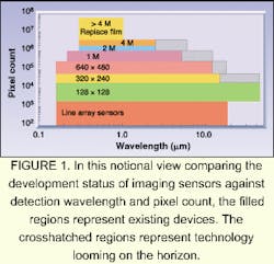
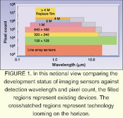
For the last two decades, the charge-coupled device (CCD) has been the preferred solid-state imaging sensor for visible applications because it can detect, store, delay, and read out an analog signal with relatively low noise and high uniformity. Even today's most sensitive visible-light cameras often use CCDs. While this popularity is a consequence of the long-term proven performance of these devices, the dependence on CCD technology for low-light-level imaging currently forces several compromises. As a result, scientists are also evaluating other options (see Fig. 1).
A CCD for low-light-level applications will typically have relatively large pixels (coarser resolution than available with consumer cameras) to collect more light. In addition, when the selected device has only one or few video outputs, it also is constrained to slow frame rates. Lowering the frame rate and the concomitant signal bandwidth essentially serves to maintain or improve the signal-to-noise ratio by overcoming the CCD output amplifier's white noise.
Using this strategy, astronomers have successfully lowered CCD read noise to one electron at video bandwidths of several tens of kilohertz, with the resulting frame rates mainly useful for viewing static scenes such as dim celestial objects. Consumer products, on the other hand, have used near-infrared light to illuminate the scene, instead of solving the problem.
Read noiseOne useful parameter for comparing the performance of low-light-level imagers, including CCDs and competing complementary-metal-oxide-semiconductor (CMOS)-based devices, is read noise. Since buried n-channel CCD technology has dominated the low-light-level application area, the read noise is often expressed in units of carriers (the type of signal collected in the imager).Currently, there is an inevitable trend toward higher read noise at higher frequencies unless there is an amplification stage in sequence before the output amplifier. For this reason, the key questions being addressed by many researchers today are where and how to amplify.
Both fundamental and practical considerations lead to higher read noise at higher frequencies. Fundamental white noise in the unity-gain CCD output amplifier limits performance, since cooling to reduce it would be expensive and power consuming. In addition, the output impedance of a CCD output driver exceeds 100 Omega, which is not ideal for driving video signals. Output impedances this high in systems operating at megaherz frequencies will result in noise pickup from ringing and feed-through. Everywhere else, though, video drivers unencumbered by technological and power considerations will feature driving and receiving impedances of 75 Omega.
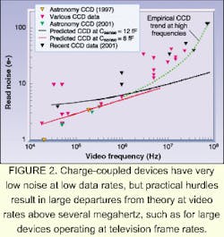
There are theoretical limits for CCD read noise at or near room temperature for sense node capacitances of 8 fF and 12 fF. These detectors have very low noise at low data rates, but practical hurdles result in large departures from expected readings based on theory at video rates exceeding several megahertz (see Fig. 2). Many video CCDs have sense capacitances within this range for converting the CCD charge into an output voltage. Assuming that one electron is transferred from the CCD channel to the sense capacitance, the maximum resulting signal voltage is a miserly 13.3 µV for a capacitance of 12 fF.
With 25-MHz video at an aggressive bandwidth of 50 MHz, the noise spectral density at the output must be very low (approximately 2 nV/Hz0.5) to match the 1-electron signal generated by each photon with 1 electron of noise, let alone allow robust detection of single quanta with subquantum noise. Switching to multi-output CCDs and using image processing to suppress the fixed pattern noise generated by video amplifier mismatch helps CCD-based cameras move to higher frame rates with lower temporal noise than otherwise readily achievable. Researchers, however, often prefer alternatives for boosting the signal-to-noise ratio that amplify the detected signal above the CCD camera's noise floor.
For example, a real-time video display of 2 million pixels at a 30-Hz frame rate equates to a video rate of nearly 100 MHz. Configuring such a CCD sensor with several hundred output taps to limit the read noise to a few electrons essentially places the CCD designer in the world of the CMOS active-pixel-sensor designer. The only problem is that there is no access to the same tools for low-noise signal processing on the focal plane.
Amplifying the photo-generated signal prior to the CCD also can enhance CCD-based camera performance. Optomechanically coupling a video CCD to a microchannel plate, for instance, amplifies the incoming photons above the read noise of the video CCD.
Another alternative for preamplification is the electron-bombarded CCD, which couples a photocathode to a CCD in a vacuum enclosure. Because an electron-hole pair is created for every 3.6 eV of input energy, this type of system accelerates photoelectrons emitted from the photocathode directly into the CCD pixels with gain. By supplying hundreds to thousands of volts, the process highly amplifies the detected signal prior to multiplexing in the CCD.
The most recent signal-boosting enhancement involves amplification within the CCD. One option that has worked for advanced CCDs is avalanche multiplication using a second output register with avalanche gain between the normal serial register and the CCD sense node.1 Even with uniform and linear gain quite high, the effective read noise is negligible, but this benefit comes with some trade-offs.
CMOS-based sensors enter the pictureWhile the preceding CCD-based schemes work in specific applications, the question must be raised about whether CMOS detectors can provide the signal amplification. Such technology already provides high gain with low noise and low power in many integrated circuits, including modern analog/digital converters. Even designers of infrared (IR) focal plane arrays began migrating from CCD readouts to CMOS multiplexer technology in the mid- to late-1980s.Although many available low-light-level cameras still exploit CCD sensor technology for signal readout, the pixel-based amplification provided by deep submicron CMOS technology is now facilitating a similarly disruptive migration for visible and near-IR sensors. For fundamental reasons, CMOS-based imagers can offer lower temporal noise at video rates, while also providing on-chip integration of camera-related functions.2
Temporal noise is lower because the vital signal bandwidth is orders of magnitude smaller. This advantage is fueling the development of both monolithic and hybrid imaging sensors with CMOS amplification. The monolithic devices have architecture similar to the venerable CCD except that each pixel amplifies the detected signal prior to the multiplexing stage. The hybrid devices, on the other hand, are vertically integrated multichip modules that use CMOS amplifying and multiplexing readouts in partnership with either silicon positive-intrinsic-negative (pin) detectors or alternatives that use other materials and structures with different band gaps. These can be wider to reduce dark current and raise operating temperature or narrower to detect at longer wavelengths.
One benefit of the hybrid approach is the capability for independent optimization of the optical fill factor and the detector amplifier design, which is possible because signal detection and readout are segregated. This type of multichip module performs quantum detection in a detector array specifically optimized for the desired spectral band. The low-noise signal amplification and image processing are performed with a CMOS readout. The mechanical and electrical interface usually relies on indium interconnects.
A hybrid manufacturing approach hence allows optimizing, both the CMOS readout and the detector to the extent possible with current processes. Hybrid silicon-to-CMOS sensors, for example, provide quantum efficiency exceeding 80% across a broad wavelength range from about 350 to 920 nm with 100% fill factor and low dark current.
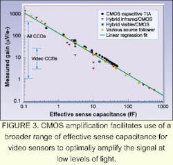
Unlike with CCDs, in which charge-to-voltage conversion and video signal buffering occur in the output stage, CMOS devices separate these critical functions so that gain is optimized for each application (see Fig. 3). The effective sense capacitance for CMOS sensors ranges from about 0.1 x 10⁻¹⁵ F to several pF with corresponding conversion gain exceeding 1 mV/e- for large format video, which is typically more than 10 times higher than competing CCDs.
Performance measuresTo help compare the performance of electronic imaging sensors to both photographic film and electronic sensors with different pixel size and performance attributes, the International Organization for Standardization (ISO) has specified standards to help system users obtain proper exposures and determine the low-light capability of photographic and electronic still cameras.While not a perfect solution, the ISO speed rating is still a good benchmark for video since many video cameras now capture and display still imagesmaking the rating an important figure of merit for all imaging systems. If a photographic film camera has an ISO rating of 1000, then the same aperture and exposure time used for the film camera should be appropriate for an electronic camera with that rating.
In daylight scenes, film with an ISO 1000 rating requires a shutter speed of 1/1000 of a second to take a good photograph at f/16 lens aperture. Just as there are many types and speeds of photographic films, there are also many competing solid-state devices such as CCDs or CMOS imaging sensors. Furthermore, CMOS imaging sensor technology spans many incarnations including hybrid and monolithic embodiments that use active pixel sensor schemes or competing imaging system-on-a-chip architectures.
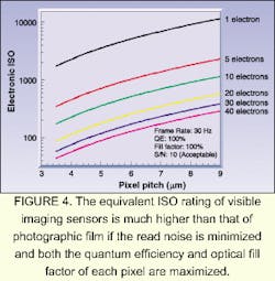
To facilitate comparison of detectors, it helps to examine theoretical plots of the equivalent electronic ISO rating as a function of pixel pitch for read noise ranging from 1- to 40-electron signals (see Fig. 4). Specifically shown in Fig. 4 are estimates for a signal-to-noise ratio of 10, a level corresponding to the "first acceptable image" criterion for quality according to ISO Standard 12232.3 Other assumptions include a 30-Hz frame rate, square pixels, 100% quantum efficiency, and a 100% optical fill factor. The quantum efficiency and fill factor of specific imagers, however, can be significantly lower.
Based on these data, a megapixel CCD-based camera with pixels approaching 5 x 5 µm and read noise of 1 electron likely has electronic ISO rating somewhat lower than the maximum value of about 3000. This is because both the fill factor and quantum efficiency are below 100%. The device also would operate at frame rates significantly lower than 30 Hz. At full video rates, today's CCD-based video cameras thus often have ISO quality well below 100 at a 5-µm pixel pitch even though the technology is extremely mature.
Though still at an early stage in development, CMOS megapixel sensors already exceed several hundred ISO rating units at frame rates compatible to television. Using advanced noise reduction techniques that lower read noise to below 1 electron at full video rates even for large arrays, CMOS advocates are betting that CMOS will eventually be the final answer for such applications.4, 5 ISO speeds greater than 3000 and 10,000 are possible at pixel pitches of 5 and 9 µm, respectively.
REFERENCES
- A. Wilson, Vision Systems Design (October 2000).
- L. J. Kozlowski, J. Luo and A. Tomasini, IEDM Proc. (1999).
- Final Draft International Standard ISO 12232, "PhotographyElectronic still picture camerasDetermination of ISO speed" (Oct. 10, 1997).
- B. Fowler, M. Godfrey, J. Balicki and J. Canfield, Proc. SPIE 3965, 126 (May 2000).
- European Patent EP988749A1, "Compact Low-Noise Active Pixel Sensor with Progressive Row Reset" (March 29, 2000).
LESTER J. KOZLOWSKI is a researcher with Rockwell Science Center, 1049 Camino Dos Rios, Thousand Oaks, CA 91360; e-mail: [email protected].