Video recording captures fast-moving targets
Gordon W. Kent
Advances in CMOS sensors with on-chip circuitry for high-speed digital imaging have made digital video competitive with film, and even superior to it on several fronts.
For most of the past century, high-speed imaging in one form or another has been a valuable tool for analyzing motion too rapid to be seen by the unaided eye. Although the methods of recording the images have changed drastically over time, the goal has remained the same. Film-based imaging remains the recording medium of choice for many specialized high-speed applications. Electronic recording devices, however, have gained in popularity since standard video cameras were modified in the 1970s with mechanical rotating shutters to reduce image blur. More recently, systems have emerged that are designed exclusively for high-speed recording, supplying frame rates many times faster than standard commercial video recording speeds in the United States and Europe (NTSC /PAL).
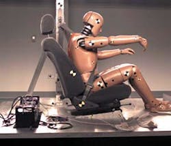
The first high-speed video systems were large and expensive, requiring special recording tape and bulky recorders. Image quality was lacking, and they were not user friendly. Because of these limitations, early systems were primarily used in areas such as auto testing, weapons testing, and exotic research. The latest high-speed video cameras have gone digital, and now are relatively common in almost any environment. The new generation of digital high-speed video systems has eliminated many of the shortcomings of their predecessors. The quality and speeds offered by these systems are beginning to rival film in many respects (see Fig. 1).
A technician can now visually troubleshoot a mechanical assembly on the production floor, do quick motion analysis, and transmit images and data to other facilities within minutes of recording. This is all possible without the resources of an in-house department staffed with photo technicians and specialized equipment. With some current configurations, a small camera unit and a laptop computer constitute the major components of the system.
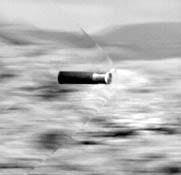
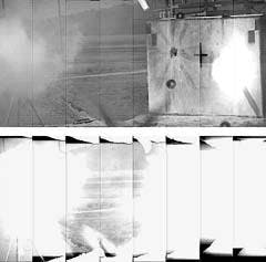
Color or monochrome designs offer variable full-frame recording rates of up to 1000 pictures per second (pps) via complementary metal-oxide semiconductor (CMOS) or charge-coupled device (CCD) sensors (see Fig. 2). Sensors vary by camera model in sizes ranging from approximately 500 x 500 to more than 1000 x 1000 pixels. Speeds as high as 60,000 pps are possible using a smaller operator-selected portion, or "windowed" area of the full sensor (see Fig. 3). In addition to rapid frame rates, digital systems are also equipped with electronic shuttering that controls the exposure time of each image, as short as 5 µs, to reduce or eliminate image blur. Cameras also can be synchronized with pulsed lasers to trigger the laser for each exposure, or the laser's pulse signal can be used to control the camera to trigger each individual exposure.
Digital high-speed equipment is a major investment compared to standard video camera systems, but prices have decreased over the last several years, especially considering new advanced capabilities and money values. A digital high-speed camera system can literally pay for itself in saved material, production down time, and wasted test and research resources during one photo session.
A major factor in current high-speed advances is the switch from CCD image sensors to CMOS. The CCD remains the sensor of choice in high-end imaging devices for applications that don't require high-speed recording rates. The CCD offers outstanding resolution with low noise and very good linear response. But CMOS sensors offering features that include on-chip multiple sampling, amplification high-speed imagings, and n-well fabrication compare well with older CCDs in terms of noise, fill factor, linearity, dynamic range, and sensitivity.
The image quality now possible with CMOS is great news for the designer of a high-speed video camera. Many of the early high-speed cameras used multipanel, multitaped CCD sensors. These sensors were actually a composite of multiple sensors combined on a single chip to increase readout speeds providing higher frame rates than possible with conventional sensors. These multiple imaging segments were difficult to accurately balance. They also consumed a considerable amount of power, and were expensive.
Reduced blooming
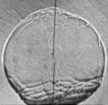
Overexposed areas of an image can cause an expanded halo or wash-out effect that can obscure important details in a scene (see Fig. 4). This "blooming" problem is one of the primary shortcomings of CCD sensors expressly designed for high-speed use. Lighting conditions can be extreme in many applications, and bright reflections on polished metal or glass surfaces, missile exhaust plumes, and explosive subjects can overload CCD pixels causing the excessive charge to bleed into adjacent pixels. This effect can be extreme, sometimes bringing out the physical structure pattern of multipanel sensors and greatly degrading image quality. The design structure of a CMOS sensor is virtually immune from this blooming effect even when heavily overexposed.
Physical camera size is always a design consideration, and smaller is better. Another primary advantage of CMOS technology is the very low power required for operation; the less power consumed by the camera head, the smaller it can be. Multiple off-chip control components required by CCD sensors use multiple voltage inputs The CMOS sensor runs on a single, low-voltage supply that can cut power input requirements and resulting heat dissipation from 20 to 100 times. Some older CCD systems have been known to quit unexpectedly in hot environments. Low power consumption helps prevent this problem, with the added advantage of extending battery life in field environments.
The CMOS active pixel sensor (APS) construction now makes it possible to include circuitry on the chip, at each individual pixel. Some of these added circuits replace separate off-chip components needed with CCD systems, and they also make new on-chip options possible. This "camera-on-a-chip" circuitry has supplied high-speed camera designers with a whole new bag of tricks for truly useful camera high-speed imagings.
Reliable and accurate "snap shot," or "global," shuttering provides control of integration time to all of the pixels on the chip at exactly the same time. Previous CMOS designs used a "rolling" shutter that exposed each row of pixels at a slightly different time during the total integration period. This shuttering method can result in skewed data for moving subjects. Examples of this rolling shutter effect include elongated tires on early race car images, or the golf club shaft that appears to bend upon ball impact. The rolling shutter can also present problems when extremely short strobe or laser pulses are needed.
On-chip circuitry can also supply automatic pixel-level control of exposure. Such an "extended dynamic range" high-speed imaging sends an early reset pulse to overexposed pixels during the integration period. These drained pixels then continue collecting photons for the rest of the exposure. The other darker pixels continuously build a charge for the entire exposure. This high-speed imaging optimizes scenes with extreme contrast, allowing full exposure of dark areas in the scene while reducing overexposure in the very bright areas (see Fig. 5).
Unlike film- or tape-based recorders, digital high-speed systems can be left unattended for extended periods of time, waiting for a trigger to record an unpredictable event. In this standby mode, new images are continuously sent to the camera memory while old images are flushed out. When the trigger is initiated, images are permanently stored to the memory.
Recorded image sequences can be played back directly from RAM and archived to the controlling computer's hard drive or other external storage. These image files can be quite large, and the use of the rapid IEEE 1394 data interface (such as FireWire) speeds transfer times. This data interface supports the control of up to 63 cameras from one computer control system.
Looking forward
The sensor of choice for the future will continue to be CMOS, and higher-resolution designs will appear, along with faster recording speeds. High-resolution megapixel sensors are available now. Designing and manufacturing higher-pixel-count sensors is not difficultthe more perplexing design challenge is how to read, store, and transfer data.
One of the most intense areas of high-speed research is the development of real-time data transfer and extended recording times. Extremely rapid real-time compression and data transfer to external storage is the key to many new high-speed imagings, and the next serious hurdle to overcome.
GORDON W. KENT is sales manager at Vision Research Inc., 190 Parish Drive, Wayne, NJ 07470; e-mail: [email protected].


