Position sensors provide multidimensional precision
While charge-coupled devices (CCDs) and complementary metal-oxide semiconductor (CMOS) detectors offer excellent imaging ability, neither technology provides the response speed required for many scientific applications. In addition to the faster response times, these applications also often require precise positioning data. This demand continues to fuel research in position-sensitive detectors (PSDs).
Basic device types
Although there are essentially three basic types of PSDs, there can be several variants within each category. Either the detection and amplification take place in a vacuum, as with photomultiplier tubes (PMTs), or in a gas, or in the solid state. Position-sensitive PMTs, for example, multiply the electrons produced by photons within electrodes in an evacuated chamber. Position-sensing capability comes from using multiple anodes to collect the electrons or by amplifying the electrons in narrow microchannels, each representing a single pixel. Alternatively, fine-mesh electrodes can be used to keep the elections moving in straight lines, which allows localizing their position of origin. In some designs, the location of the electrons is read out through an array of crossed wire grids that provide positioning feedback for each electron striking a grid.
The second PSD category encompasses gas amplifier detectors, which typically find use in x-ray detection, mainly for energy ranges below 20 kV, where the radiation can be absorbed in a few centimeters. As in a PMT, an x-ray photon knocks an electron off an atom, which, once accelerated by an imposed electrical field, knocks off more electrons and starts an amplification avalanche. Each photon can produce millions of electrons in this manner.
To use gas amplification for position-sensitive detectors, though, the avalanche must somehow be localized and read out by separate anodes. This can be done using a microstrip gas chamber, which uses a sequence of alternating thin anode and cathode strips on an insulating support, typically glass. The pitch is generally around 100 to 200 µm. One problem with this approach is that charge can accumulate on the surface of the glass, which can then affect the amount of gas amplification, leading to instabilities.
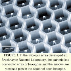
An alternative arrangement is based on the micropin array developed at Brookhaven National Laboratory (Uptown, NY).1 The device has a hexagonal array of cathodes and anodes generated by lithographic techniques (see Fig. 1). The cathode is a connected array of 48 × 56 hexagons, each with a radius of roughly 300 µm. Anodes are recessed 50-µm-wide pins in the center of each hexagon. Since the accelerating field is between each anode and the surrounding cathode, each x-ray photon produces an avalanche that travels toward the anode nearest to the atom that absorbed the photon. The spatial resolution is thus 300 µm.
According to Brookhaven researchers, the detector can easily grow to a 1000 × 1000 array. The short accelerating region also leads to a fast response time, which allows the detector to count photons at a rate of almost 100 MHz.
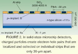
Microstrip solid-state detectors, which make up the third common PSD category, find use in charged particle detection (see Fig. 2). In these devices, silicon-dioxide strips alternate with aluminum-conducting strips. Typical pitch is 20 µm. The aluminum strips sit on top of p-doped silicon layers, which in turn overlay a much thicker n-doped silicon layer. In one dimension, position accuracy is thus very high, and response times can be faster than 5 ns. In silicon detectors, however, there is no charge amplification, so high-energy particles only produce 30,000 or so electron hole pairs and require very low-noise electronic amplification.In semiconductor detectors, an ionizing particle penetrates the detector and produces electron-hole pairs along its track, the number being proportional to the energy loss. An externally applied electric field separates the pairs before they recombine. As a result, electrons drift toward the anode, holes to the cathode. The charge collected by the electrodes then produces a current pulse on the electrode, which is a measure of the deposited energy. The readout goes through a charge-sensitive preamplifier, followed by a shaping amplifier. Because silicon detectors are asymmetric p-n junctions, to work as a detector, though, the p-n diode must be reverse-biased by applying a positive voltage on the rear ohm contact (a metal deposited on the n side).
The good energy resolution is attributable to the low energy threshold. Only 3.6 eV are necessary to produce an electron-hole pair—which is relatively low compared to the 30-eV ionization energy in a gas or the approximately 300 eV necessary to extract an electron from a photocathode coupled to a plastic scintillator.
Several research groups have developed solid-state PSDs that rely on something called the lateral photoeffect. When a photon is incident on the surface of a planar p-n junction, it produces a photopotential along the length and across the width of the junction, causing current to flow laterally towards the electrodes at the edges of the junction.
The potential difference between the bindery electrodes depends on the distance between the point where the photons arrive and the electrodes. As with the crossed-wires PMTs, the location of each arriving photon can be determined using the changes in the observed potential. Such PSDs work best when there is an optical beam to be localized, rather than an image to be created.
In some solid-state devices, it is possible to measure the position of incoming photons in three dimensions (3-D), not just two. For example, 3-D gamma-ray detectors developed at the University of Michigan's Department of Nuclear Engineering and Radiological Sciences (Ann Arbor, MI), can measure both interaction depth within a cadmium zinc telluride (CdZnTe) detector and the location of the photon absorption in the other two dimensions.2 Such accurate depth information can be useful in applications that use gamma rays to image and test opaque materials for defects or uniformity.
Using a 1-cm cube of material, the gamma-ray device can measure the ratio of the signal produced by each photon at the cathode to that produced at the anode. For the most part, the cathode-to-anode ratio is proportional to the depth of the interaction, so the depth to be calculated from the ratio. The anode is broken up into 2-D pixels to provide localization in the plane perpendicular to the depth direction.
Applying position sensing
In general, PSDs find use in applications detecting x-rays, gamma rays, and charged particles, although the devices sometimes also apply in the optical range. A major application involves positron emission tomography. Here, radioactively labeled substances concentrate where the activity of interest, such as oxidation, takes place. This allows researchers to study these activities in real time.
In such devices, the radionuclides emit positrons, which rapidly collide with and annihilate electrons, producing pairs of oppositely-directed gamma rays. A ring of PSDs records the gamma rays. Coincidence counting circuits define the line along which the gamma rays emerged. Mapping many such scintillations allows building a 3-D map of the radionuclide concentration. In addition, researchers can measure the time of flight to each scintillator, which also allows determining the distance along the line connecting the detectors.
Position-sensing devices also find use in astrophysics. For example, satellite-borne gamma ray and x-ray observatories are becoming increasingly sophisticated in gathering, and, in the case of x-rays, focusing high-energy radiation from hot sources in the universe, from quasars to vast clouds of plasma. PSDs allow recording the images and determining detailed time resolution.
In high-energy physics, another key application area, large PSDs surround the interaction regions where relativistic particle from accelerators slam into targets, producing showers of daughter particle and high-energy gamma rays.
Future PSD potential
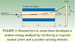
With ongoing advances in PSD technology, researchers are creating new instruments to measure not only gamma and x-rays properties, but those of particles as well. For example, scientists at the Institute of Physical and Chemical Research (RIKEN; Satama, Japan) have developed a neutron energy analyzer by combining a magnetic neutron prism and a PSD.3
The magnetic prism uses a quadruple magnetic field created by four magnets (see Fig. 3). Neutrons, while they have no charge, do have a magnetic moment, so are diverted by the magnetic field gradient created by the quadruple magnet. The higher the neutron energy level, the less intense the diversion, so the neutrons spread out into a spectrum. When they arrive at the PSD, they collide with a suitable scintillator material, producing x-rays that can then be detected by a position-sensitive PMT or other type of PSD.With applications in the medical and research fields driving PSDs to even higher performance, this field is likely to remain a rapidly moving research area for some time.
REFERENCES
- P. Rehak et al, IEEE Trans. Nuc. Sci 47, 1426 (August 2000).
- W. Li et al, IEEE Trans. Nuc. Sci 47, 890 (June 2000).
- T. Oku and H. M. Shimizu, Physica B 276-278, 112 (July 2000).
About the Author
Eric J. Lerner
Contributing Editor, Laser Focus World
Eric J. Lerner is a contributing editor for Laser Focus World.


