Multi- and hyperspectral detectors transform sensing
Just as color images contain far more useful information than black and white ones, multispectral and hyperspectral detectors with multiple wavelength bands provide more information than conventional three-color images. Often, they extend beyond the visual range into the infrared (IR) or the ultraviolet (UV)—sometimes sensing in both directions at once. Such detectors offer sensitivity to the degree that users can distinguish individual species of trees from space or even identify moving, camouflaged tanks from great distances.
Splitting it up
The most widespread approach to multispectral detectors involves splitting the incoming radiation with filters and then focusing the various spectral bands toward separate detectors. One example of this approach is the Multispectral Thermal Imager Satellite (MTIS), which was launched at the end of 1999 with the goal of studying industrial facilities and related environmental impacts from space.1, 2 Its core is a multispectral sensor consisting of linear detector arrays that have optical filters placed immediately above them in the focal plane of a telescope. The arrays, one for each required spectral band, line up along the track of motion of the satellite. As the satellite moves, a given image scans across each array in turn, allowing the system to build a two-dimensional (2-D) multispectral image.
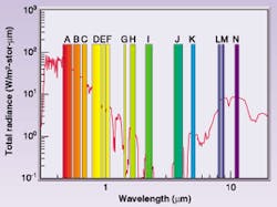
The MTIS uses 15 bands ranging from a band of 450 to 520 nm to a band of 10.2 to 10.7 µm (see Fig. 1). It takes three separate multispectral arrays to cover the full 30-mm width of the device's focal plane. Each array uses three different detector materials to access the various wavelengths—silicon photodiode for visible wavelengths (450 to 860 nm), indium antinomide for near- and mid-IR (860 nm to 5.07 µm), and mercury cadmium telluride for the long wavelengths up to 10.7 µm.
The sensor chip assemblies contain photodetectors that are attached by indium electrodes to readout integrated circuits, which amplify and store the signals from each pixel. The resolution varies, depending on the wavelength. For the visible bands, 828 pixels are used, each 12.4 µm across, but for the IR bands, there are 207 pixels, each 49.6 µm across. These sensor characteristics allow a 5-m resolution for visible and a 20-m resolution for IR data spanning a width of 12 km.
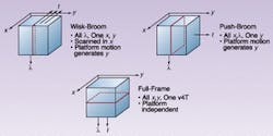
For most space-based multispectral or hyperspetral sensors, the motion of the observing platform accounts for one of the scanning directions (see Fig. 2). In other multispectral applications, devices can provide information related to four dimensions—two spatial dimensions, wavelength, and time. For example, in real-time hyperspectral imaging, images are obtained at a video rate. Such imagers must therefore be able to scan in both spatial dimensions and produce vast amounts of data. For instance, the multiband indentification and discrimination imaging spectrometer (MIDIS) system under development by US Army Armament Research and Development Engineering Center (Picatinny Arsenal, NJ) and Surface Optics Corp. (San Diego, CA) generates more than 130 Mbyte/s.3Dual-band detectors
Whenever multispectral arrays of the type described here are used, multiple arrays, filters, and in many cases, beamsplitters, add to device complexity, alignment problems, and cost. These issues are fueling research efforts to develop and fabricate single arrays with multiband capabilities integrated into each individual pixel. It may be impractical to integrate many bands into a single pixel, so hyperspectral imaging cannot use this approach, but research on two-band structures is very active, and three- and four-band structures may be possible within the decade.4 Dual-color detectors now in development are based on mercury cadmium telluride (HgCdTe) photodiodes and quantum-well IR photodetectors (QWIPs). The latter devices are easier to fabricate with high yield. They also have a larger industrial base. The former ones have higher quantum efficiency and operating temperatures, as well as the potential for higher performance overall.
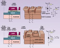
In either approach, the dual-band detector consists of a longer-wavelength detector behind a shorter-wavelength one so that the long-wavelength radiation passes through the first detector and is recorded by the second. For HgCdTe devices, the detector is an n-p-n triple layer heterojunction consisting of back-to-back p-n junctions (see Fig. 3). In the simultaneous-mode design, there is an additional electrical contact to the center layer that allows reading out each layer independently. In the sequential mode design, the readout selects each layer and therefore each wavelength band through a change in the bias voltage.The sequential approach has several advantages related to the fact that it only requires one readout connection per cell. This translates into smaller, more-reproducible unit cells and a nearly 100% fill factor. Nevertheless, since the construction of such devices does not allow independent selection of the optimum bias voltage for each layer, there can be substantial mid-wavelength crosstalk in the long-wavelength detector. The simultaneous mode avoids this problem, but at the expense of greater complexity.
A key technical issue in dual-layer detectors revolves around high dislocation densities. The cadmium zinc telluride (CdZnTe) substrates are matched to the lattice spacing of the long-wavelength IR HgCdTe layer. When the mid-wavelength IR HgCdTe layer, with a different ratio of Hg to Cd, is deposited on the substrate in dual-color devices, there is a small (0.04%) lattice mismatch, resulting in a higher density of dislocations.
Despite the difficulties, several companies plan to market simultaneous-mode dual-band technology in larger array sizes in the near future, while development efforts continue to increase the number of bands covered to three or four.
Multispectral QWIPs
The main alternatives for multicolor devices are quantum-well IR photodiodes (QWIPs). Here, the dopants are concentrated into microscopic regions, creating quantum wells in which the band structure has shifted. Detection occurs when a photon knocks an electron or hole out of the quantum well into the neighboring band. Like HgCdTe detectors, dual-band detectors can be created by stacking long- and medium-wavelength QWIPs, each comprising repeated layers of indium gallium aluminum arsenide (InGaAlAs) surrounded by layers of indium gallium arsenide (InGaAs) and indium aluminum arsenide (InAlAs). With only one set of contacts, the observed wavelength depends on the voltage bias, with low voltage activating the long-wavelength detector and high voltage activating the mid-wavelength device to allow sequential readout. In such a detector developed at Northwestern University (Chicago, IL), for example, a 5-V bias has detection sensitivity peaking at 8 µm, and a 10-V bias has sensitivity peaking at 4 µm.5
Applying multispectral detectors
In addition to broad surveys from space, multispectral and hyperspectral detectors have potential applications in environmental and defense areas. For example, a hyperspectral imager developed by the Michigan Technical University (Houghton, MI) and Kestrel Corp. (Albuquerque, NM) is surveying the ecosystem of Lake Superior and the surrounding area with very fine spectral resolution. This allows researchers to perform such tasks as assessing the origins and extent of water flows into Lake Superior, tracing sediments, monitoring dissolved organic matter, and tracking biomass and tree health for individual tree species, such as aspen, white birch, red pine and hemlock.
The Army's MIDIS (multiband identification and discrimination imaging spectrometer) system, for example, has a variable spectral resolution reaching up to 128 bands. This allows scanning an area in real time for specific spectral signatures or even for a specific spectral signature related to something that is in motion. With high spectral resolution, a vast variety of objects have specific colors, which facilitates object recognition. Instead of looking for the shape of a tank, which changes depending on the viewing direction, the scanner can look just for the specific spectral signature as if it were looking for the only red object in a scene. Combining spectral tracking with motion sensitivity makes object detection even easier.
To illustrate the sensitivity of MIDIS, researchers compared the spectral signatures of soil before and after a mine had been buried in it. By correlating the spectrum from a given scene with the spectrum from a known buried mine, the team could locate an array of 12 mines precisely.
The same technology also has potential in a variety of civilian applications, including detection of malignant tumors, quality control, and mineralogical searches. Such applications are already becoming reality and will likely see more widespread use within the next five years.
REFERENCES
- J. Rienstra and M. Ballard, SPIE Proc. 3753, 369 (January 2000).
- P. G. Weber, SPIE Proc. 3753, 340 (Jan. 2000).
- M. Dombrowski and P. Wilson, SPIE Proc. 3753, 100 (January 2000).
- A. Rogalski, Infrared Physics and Tech. 41, 213 (August 2000).
- J. Christopher et al, SPIE Proc. 3629, 147 (July 1999).
About the Author
Eric J. Lerner
Contributing Editor, Laser Focus World
Eric J. Lerner is a contributing editor for Laser Focus World.


