Newsbreaks
Voltage-tunable superlattice IR detector has low dark noise
Two-color IR photodetectors, often with detection bands in the 3- to 5-µm and 8- to 12-µm wavelength regions, are useful for remote measurement of temperature. One approach to providing two detection bands is voltage tunability between the bands; however, technologies developed thus far to do this result in high dark currents that raise the background-limited temperature. Now, researchers at Princeton University (Princeton, NJ), the U.S. Army Research Laboratory (Adelphi, MD), and Sandia National Laboratories (Albuquerque, NM) have created a voltage-tunable two-color superlattice IR photodetector (SLIP) with a background-limited temperature comparable to those of single-color quantum-well IR photodetectors.
Two different superlattices are designed for mid-wave IR (MWIR) and long-wave IR (LWIR) detection; a thick blocking barrier prevents high dark currents. Multiple superlattice pairs are fabricated. A voltage bias of greater than 0.6 V produces a peak response at 9.1 µm, while a negative bias shifts the peak to 3.9 or 5.2 µm depending on the voltage. The background temperature for LWIR detection is 70 K, while for MWIR it is 110 K. The two-terminal layout enables the fabrication of large, low-cost focal-plane arrays. Contact Amlan Majumdar at [email protected].
Simple photonic crystal tailors thermal emission
As was demonstrated at Sandia National Laboratories (Albuquerque, NM) in 2003, 3‑D photonic crystals can be used to tailor the emission spectra of thermal sources (see Laser Focus World, December 2003, p. 93). The intricate Sandia structure, made of tungsten, can be heated to very high temperatures and has the potential of improving the efficiency of incandescent-lamp filaments. For low-temperature IR uses, however, lower-cost approaches to creating emission-tailoring PCs might be preferable.
Researchers at CNRS (Marseille, France) have developed just such an approach, in which layers of microstructured gold films are alternated with uniform films of zinc selenide (ZnSe). The 30-nm-thick gold layers are patterned with grids of circular holes approximately 1.5 µm in diameter on a 2.9-µm pitch; the ZnSe layers are 1.1 µm thick. An experimental device with five pairs of layers was fabricated. A theoretical transmission spectrum shows a bandpass behavior with a long-wavelength cutoff of about 12 µm; experimental measurements are roughly similar. Emissivity of the coating peaks at 7.9 µm and is somewhat directional. Possible uses include making objects “stealthy” at IR wavelengths. Contact Stefan Enoch at [email protected].
High-brightness white OLED demonstrates 25-lm/W efficiency
A collaboration between Philips Lighting (Eindhoven, The Netherlands) and Novaled (Dresden, Germany) has yielded record efficiency for a high-brightness white organic light-emitting diode (OLED). By combining Philips’ layering techniques and optical outcoupling with Novaled’s doping technology, the researchers were able to achieve 25-lm/W power efficiency at a brightness level of 1000 cd/m2.
The small-molecule, top-emitting p-i-n OLED combines red, green, and blue emitters and utilizes various proprietary materials, including Novaled’s p-dopant (NDP-2), to achieve the higher power efficiency. According to Novaled, the p-i-n design is critical to achieving OLED efficiencies of 100 lm/W at 1000 cd/m2, which is considered necessary for OLED lighting to become practical. In addition, the p-i-n design allows for more cost-efficient production due to the wider variety of substrates and electrode materials that can be used. While the operational lifetime of this white OLED is not yet that of other Novaled OLEDs (100,000 hours for red, 50,000 for green, 6000 for blue at a 500 cd/m2 starting brightness), the company is working to develop new transport materials to enhance temperature stability (to above 100°C), efficiency, and lifetimes. Contact Jan Birnstock at [email protected].
EDFA achieves 94-nm bandwidth
Conventional erbium-doped fiber amplifiers (EDFAs) are typically designed for C- or L-band operation from about 1530 to 1560 nm or 1560 to 1610 nm, respectively. By using longer erbium-doped fiber lengths, or through Raman amplification and different hybrid amplifiers, a wideband C-to-L amplifier has also been reported. Now, scientists from National Chiao Tung University and the Industrial Technology Research Institute (both in Hsinchu, Taiwan), Chungwa Telecom Company (Taoyuan, Taiwan), and Yuan Ze University (Chung-Li, Taiwan), have demonstrated a coupled-structure S-to-C-band amplifier with a 94‑nm gain bandwidth from 1476 to 1570 nm.
To achieve wideband operation, the coupled-structure amplifier was constructed from an S-band EDFA module composed of two EDFA stages and a power-sharing 980-nm pump. Two wavelength-division-multiplexing couplers were used to connect the S-band module to a C-band erbium-doped waveguide-amplifier module in parallel. The packaged device (including pump lasers) is 40 cm3 in size. The dual-stage gain profile showed minimum gain at 1522 nm, with a 31.4-dB peak gain and 5.6-dB noise, and a 30.5‑dB peak gain with 4.7-dB noise, at 1506 and 1532 nm, respectively, for an input signal power of -30 dBm. Contact Kui-hsiangLai at [email protected].
CMOS imager also handles free-space communication
Introduced at the 2005 Greater Cincinnati Inventors Fair in June, the patent-pending Scifeye (Cincinnati, OH) imaging sensor adds free-space optical-communication capability to CMOS imaging sensors. The simultaneous capture of visual imagery plus data from objects that transmit high-speed IR laser pulses represents the optical equivalent of radio-frequency identification (RFID). In asset-tracking applications, light-emitting tags that transmit high-speed optical data are attached to objects that pass within the field of view of a Scifeye-equipped digital camera. The sensor decodes both video imagery and identification data. Scifeye provides distinct identification and communication flow while overlaying that tracking information onto a live video feed-but without the electromagnetic interference and associated interception and jamming drawbacks of RFID.
Unlike a standard CMOS sensor, two independent busses on the Scifeye-enabled sensor allow video intensity data to be read at normal video-frame rates while communication data is read at higher rates using the supplementary bus. Each pixel in the Scifeye sensor array can receive data independent from other pixels in the array, allowing multiple data sources or optical tags in the field of view to transmit to the camera simultaneously. Contact Darryl Dieckman at [email protected].
Immersion nanogratings yield robust optical retarders
Although they have already demonstrated high-performance, zero-order wave plates such as quarter-wave (λ/4) plates and even λ/31 retarders, researchers at NanoOpto (Somerset, NJ) have now developed more-robust “immersion nanogratings” that can have their trenches filled with a variety of materials through atomic-layer deposition (ALD). The ALD process prevents the intrusion of water or contaminants into the nanograting and increases its antiscratch capability, removing major roadblocks to commercial use while allowing the deposition of a variety of filling materials that can improve optical and thermal performance.
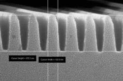
To demonstrate feasibility, the researchers first fabricated a nanograting with a period of 200 nm and a grating height of 390 nm in a BK7 glass substrate. The grating trenches were filled with a nanolaminate material composed of titanium dioxide and silicon dioxide; an antireflection coating was added as well using the ALD process (top, bare features; bottom, filled-in features). A 5.3° ±0.25° retardation was measured over a 65 × 55-mm plate area, with transmission of greater than 99.5% in the 500- to 600-nm wavelength range. Contact Jian Jim Wang at [email protected].
Gratings send blue diode laser’s light skyward
Gallium nitride (GaN)-based semiconductor lasers provide useful blue or UV wavelengths in a small package, but very high-reflectivity mirror facets are difficult to achieve. Distributed-feedback or distributed-Bragg-reflector structures beyond the end facets can aid optical feedback; as well, they can enable vertical light emission, which in turn enables on-wafer testing of the lasers. A group at the University of Bristol (Bristol, England) is fabricating blue vertically emitting laser diodes with fourth-order gratings by using focused-ion-beam etching.
The negative-detuned distributed-Bragg-reflector grating is placed in-plane beyond the laser facet and has a period of 300 nm, a tooth width of 150 nm, a depth of 160 nm, and a total of 40 periods. The laser was tested under pulsed conditions with a pulse width of 200 ns at 3 kHz. The vertical emission was monitored by a scanned probe consisting of a single-mode fiber with a lensed tip, showing that the beam had a narrow divergence. The use of nonuniform or 2-D gratings could result in fine control of beam shape, says Martin Cryan, one of the researchers. Contact Cryan at [email protected].
Silicon photodiode detects 1330- and 1550-nm wavelengths
Ordinary silicon (Si) photodetectors do not respond to the telecommunications wavelengths of 1330 and 1550 nm-in fact, Si is transparent at these wavelengths. But a silicon-microstructuring process developed by researchers at Harvard University (Cambridge, MA) has allowed them to fabricate Si photodiodes that respond to these wavelengths, which have energies that lie below the bandgap of Si.
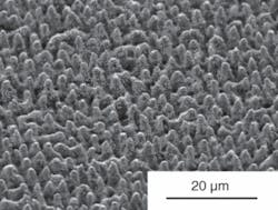
An Si wafer is irradiated with normal-incidence 100-fs laser pulses in an atmosphere of sulfur hexafluoride, and is translated so that each point on the wafer receives about 200 pulses. The resulting microstructures are 2 to 3 µm in height and width and consist of crystalline Si covered with a sulfur-containing disordered surface layer a few hundred nanometers thick; the wafer is then annealed at 825 K for 30 min. A device with an active area of 5 mm2 had responsivities of 50 mA/W at 1330 nm and 35 mA/W at 1550 nm. At 1000 nm, the responsivity reached 120 A/W, a responsivity similar to that for avalanche photodiodes, showing that the device has gain. Sulfur atoms in a nonequilibrium configuration lead to the effect, posit the researchers. Contact Eric Mazur at [email protected].
Upconversion helps silicon detect mid-IR radiation
In an effort to provide an alternative to liquid-nitrogen-cooled mid-IR (3- to 20-µm) arrays such as mercury cadmium telluride or lead selenide, scientists at the Massachusetts Institute of Technology (MIT; Cambridge, MA) are using femtosecond upconversion to allow detection of mid-IR radiation by lower-cost silicon CCD arrays.
The basis of the technique is upconversion of mid-IR radiation to the visible through sum frequency generation (SFG), a nonlinear optical mixing technique that allows detection by a standard silicon-based detector. Because previous upconversion attempts required a long, intense narrowband optical pulse with fluence in the tens of millijoules per square centimeter in order to achieve reasonable conversion efficiencies, the researchers instead use a femtosecond upconversion technique that mixes a femtosecond optical pulse with a spectrally dispersed IR pulse to generate a spatially dispersed SFG signal. This optical pulse is temporally short and requires optical fluence of only microjoules per square centimeter. Using simple optics and nonlinear crystals such as potassium and lithium niobate, the technique can be retrofitted to any IR spectrometer. Contact Matthew F. DeCamp at [email protected].


