SEMICONDUCTORS: Diamond thin film has high crystallinity
TOKYO – Under an agreement with the Japan Fine Ceramics Center, Kobe Steel has succeeded in growing high-quality diamond thin films with excellent crystalline properties. Diamond thin film is considered very promising as a semiconductor material. Because of its heat resistance, radiation resistance, and high heat conductivity, the range of possible applications of diamond is very wide.
Diamond synthesis currently involves high temperatures and high pressures, but, at less than several millimeters in size, the resulting crystals are very small. To use diamond thin films for integrated circuits, wafers greater than 25 mm in diameter are necessary.
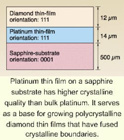
Vapor-phase synthesis is seen as a solution. Diamond thin films can be grown on single-crystal platinum; however, not only is bulk platinum expensive, it also comes in sizes only up to 10 mm, thus preventing the production of large-area thin films. The research done by Kobe Steel involves growing a platinum film on top of a separate substrate and then growing the diamond thin film on top (see figure).
Crystal growth process
A single-crystal platinum film is first vapor-deposited onto a sapphire base using the spatter method. X-ray diffraction shows that the diffraction peak in the (111) direction is much sharper than for bulk platinum, revealing the superior crystalline quality of the platinum film. Using the platinum film as a base, the diamond thin film is grown using vapor-phase synthesis. Although the resulting film is not a single crystal, the adjacent crystal boundaries are fused together so the grains are continuous. Azimuthally matched diamond (111) crystal surfaces cover the area, and the boundaries are well connected. X-ray diffraction reveals a strong peak in the (111) direction (full width at half maximum is less than 2°) and a crystal with better orientation than previously possible.
Because of the constraints of the apparatus, only a 10-mm-square base could be used. However, in principle, a larger apparatus can be used to create larger films. Single-crystal sapphire wafers up to 150 mm in diameter are commercially available, so low-cost production of large diamond films should be possible.
Further goals involve refining the process to form single-crystal films. In particular, the plan is to make the film closer to a single crystal by reducing the grain boundaries. This would be done by improving the bond between the film and the substrate and then hardening the film. Once the low-cost production of large single-crystal thin films is accomplished, the films are expected to be used in a wide range of applications such as ultraviolet light emitters and receivers and electron-emission elements.
Courtesy O plus E magazine, Tokyo
