Electrodes modulate phase of atoms
Incorporating news from O plus E magazine, Tokyo
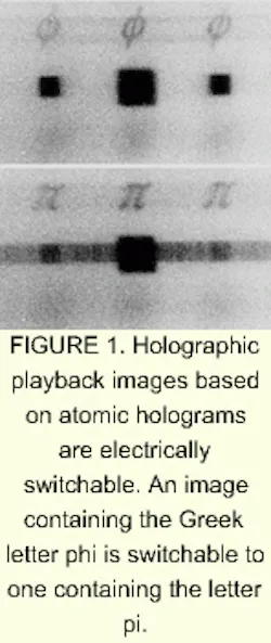
TOKYOResearchers at NEC Corp. and the Institute for Laser Science at the University of Electro-Communications have jointly created holographic playback images based on atomic holograms that can be dynamically controlled using electricity. By changing the applied voltage on electrodes positioned across the atomic hologram, the image can be converted from the Greek letter phi to the letter pi (see Fig. 1).
Atomic holography can produce nanometer-scale patterns, and it is anticipated that the patterns will be used in the production of semiconductor nanocircuits and quantum-effect components. The results of experiments show that complex three-dimensional structures can be produced by dynamically controlling the playback image.
Atoms are wavelike in the quantum-mechanical regime, and, like photons, they exhibit interference characteristics. When groups of atoms are cooled to extremely low temperatures, many of the atoms assume the same wavenumber and phase, thus emphasizing interference effects; a coherent atomic wave is produced.
In 1996, the collaborators produced proof-of-principle experiments of atomic holography using cooled atoms. For those experiments, they took the desired final image and performed reverse calculations to design the necessary holograms. For one experiment, they took a pair of comb-shaped electrodes and created a hologram with holes between the electrodes so that atoms could go through, resulting in a switching capability. The position of the electrodes and holes was calculated given the desired final phi and p shapes (see Fig. 2).
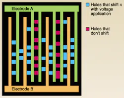
FIGURE 2. Comb-shaped electrodes modulate the phase of atoms. When electrodes A and B have the same voltage, any atoms passing through the holes do not undergo phase modulation (in relation to the phase of the atom wave). However, when a voltage is applied across A and B, the atoms going through the holes that are sandwiched between electrodes A and B (gray) undergo a 180° phase shift. Phase modulation does not occur when the holes are sandwiched between electrodes of the same side. As a result, the playback pattern changes depending on whether the voltage is switched on or off.
In this experiment, neon atoms were used. Although the atoms are electrically neutral, they have electrical-polarization properties and therefore undergo phase shifts as they progress through a static electric field. The results show, for the first time, that the phase of atomic waves can be controlled electrically.
Atomic holography recently has been in the spotlight because of the possible applications in nanofabrication. The wavelength of atomic waves is very short (less than 10 nm), so detailed patterns can be created that are not possible using optical lithography. Currently, the level of detail of the playback image is limited by the level of detail of the hologram itself. However, by using miniaturized optical systems it is possible to increase the detail of the playback image. The research collaboration is aiming to produce a playback image with resolution on the 10-nm scale. They are hoping to create three-dimensional structures using aluminum and germanium atoms in the future.
Courtesy O plus E magazine, Tokyo