CMOS SENSORS: Smart sensors yield fast and robust machine vision
Containing light-sensing elements tightly integrated with processing circuitry, image RISC processing circuitry performs tasks other vision systems can't.
Mats Gökstorp and Karl Gunnarsson
Smart-vision sensors based on complementary-metal-oxide-silicon (CMOS) technology contain photosensitive devices tightly integrated with image-processing elements on the same substrate. This arrangement eliminates the bottleneck that occurs when image data are moved serially. It also permits control of the analog properties of the sensor during the exposure. Smart-vision sensors can make possible new approaches to carrying out machine-vision tasks that are unavailable to conventional video cameras.
The first such device of this typereleased commercially in 1987was a 128-pixel CMOS line sensor that included a built-in image RISC processor; it used a separate processor element for each pixel and had a single-instruction multiple-data (SIMD) architecture. This device was followed in 1991 by a two-dimensional (2-D) device having a 256 x 256 photodiode sensor and an array of 256 processing elements, one for each column. Later developments included a 512-pixel line sensor, a 512 x 32 multilinear sensor and, most recently, a 512 x 512-pixel sensor, each with increasingly sophisticated SIMD architectures.
During their 12 years of existence, these CMOS-based smart-vision sensors have found use in many applications, from the sorting of potatoes to deployment in space. The technology has shown its strength particularly in high-speed applications, for uses requiring low power, and in harsh environments.
Architecture is highly parallel
The 512 x 512-pixel sensor array is connected to readout circuitry and to an analog-to-digital (A/D) converter that performs parallel conversion of one image row in 4-16 µs, with the length of time depending on the selected gray-level resolution (1-8 bits). Image information can be stored internally in one of 96 general-purpose registers or a group of specific registers. All of these registers have a length of 512 bits to allow one bitplane of a complete image row to be handled in parallel.
FIGURE 1. Three-dimensional profiler contains a laser and a smart-vision sensor. The laser projects a sheet of light, while the sensor detects the profile of the resulting line sweeping across a moving object. The speed of the sensor and integrated processing boosts the frame rate by thirtyfold over that of a conventional video system.
Operations on register data can be done with point, neighborhood, or global operators through dedicated logical units. The result of such an operation is placed in either an accumulator or a register or both and can be stored in any of the registers or used for subsequent operations. After each operation, the number of set positions of the accumulator is updated. This number is available in the status register. The special register group also is used for input and output. In this mode, 16 registers are altered simultaneously to produce or receive a 16-bit word at a given position along the line.
There are two buses that connect the device to external circuitry. One is the instruction bus that supplies the 16-bit instructions that control the processing. The second bus is the image input/output bus connected to the group of specific registers. Both buses are 16 bits wide. The high performance is partly related to the high degree of parallelism obtained through the SIMD architecture but is also due to the fact that four processes can run concurrently: image exposure, input/output, A/D conversion, and digital processing.
Sensor and instruction set
The photodetector is composed of a 512 x 512 matrix of pixels. The sensor is logically arranged as 512 rows each having 512 photodiodes. The lines are read out under program control to a parallel arrangement of charge amplifiers. The readout operation stores the actual photodiode charge in an analog input register that is connected to a comparator used for thresholding and for A/D conversion.
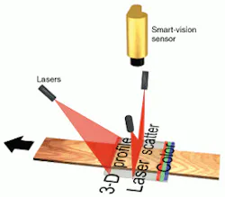
FIGURE 2. Integrated processing makes practical the sensing of many object properties at once. Separate projected light lines are configured for separate sensing purposes; one smart-vision sensor images and processes them all. Measured properties include profile, scatter, and color characteristics.
Once a specific row is defined, the analog operations are performed simultaneously on all photodiodes in that row. With this setup, the resulting charge after exposure can be read out to the charge amplifier or accumulated with previous readouts to perform analog preprocessing before digitization. In addition, because the addressing of sensor rows can be done in any order, it is possible to use different exposure times for different groups of rows.
The instruction set comprises some 80 different instructions. All of them operate on full image rows. Most of the instructions complete in one clock cycle. Some of the instructions are used to control the sensor and readout circuitry. The arithmetic is performed by three logical units: point logical unit (PLU), neighborhood logical unit (NLU), and global logical unit (GLU). The PLU instructions are bitwise Boolean operators. In the NLU, the processing of pixels is determined by the pixel's nearest neighbors to enable template matching or filtering operations. The GLU is used for global operations such as detecting or deleting the rightmost object or finding connected components between rows of data.
Processing of gray-level information is performed through bit-serial arithmetic, which uses groups of registers to hold the operands. For example, 25 cycles are needed to perform the additions of two image rows, each represented by 8-bit pixels. Because this corresponds to 512 additions along the row, an architectural advantage of more than a factor of 20 is achieved compared to a standard scalar-processor architecture such as a digital-signal processor.
Applications exploit built-in processing
Smart-vision sensors are well suited for laser range-imaging systems based on the sheet-of-light method. In such systems, a sheet of light is projected at the object to be inspected, intersecting it. An angular separation between the projected light and the axis of the CMOS sensor produces a line of light on the object having a profile that corresponds to the profile of the object. The line is imaged onto the sensor (see Fig. 1). The built-in processor detects the line and also performs necessary noise reduction (and arbitration in the case of multiple reflections). With the smart-vision sensor it is possible to obtain a frame rate of more than 2000 frames/s, as compared to a typical rate of 60 frames/s for a similar video-based system.
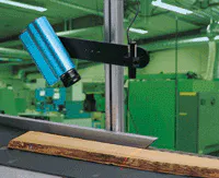
This device can be used as a multiple sensor. In this case, different areas of the sensor are used for different purposes. For example, in the inspection of lumber, one group of projected light lines can be used for range imaging while another group is used for color-separated sensing through optical filters. A third group of lines can be used together with a special laser arrangement to measure wood-cell structure by detection of scatter. This means that the same camera is able to perform several different tasks, which considerably lowers the cost of the inspection system.
The inspection of wood requires more input information than ordinary gray-scale or color images can provide. By using a smart-vision sensor as a multiple linescan sensor, a single device can provide sufficient information to achieve good grading results for different types of boards (see Fig. 2). The resulting multivariate information permits the differentiation of dirt from knots and allows detection of defects previously not possible to classify.
Another application, dispensing solder paste on printed-circuit boards (PCBs), is a very delicate step in the production of such boards and one that directly affects the overall yield and product quality. Each pad on a PCB must have an accurate volume of solder paste to ensure a secure connection to the components. Three-dimensional (3-D) inspection using laser range measurement has turned out to be a very successful way to measure and verify the volume of the solder paste. The PCBs are scanned using a relative movement between the camera-laser setup and the PCB. With smart-vision sensors, a 3-D template of the wanted volume of solder paste can be compared with each tested sample in real time.
A similar application is 3-D inspection of ball-grid arrays (BGAs). The connectors on this kind of package consist of a very large number of small solder balls in a 2-D array. For the same reasons as those for the solder-paste application, it is important to verify the shape of each solder ball. Other package types such as fine-pitch quad flat packs (QFPs) can also be inspected using this technique (a QFP is a surface-mount package with leads protruding from all four sides). By using 3-D inspection of both solder paste deposits and BGA bumps, the most common sources of faults in the production process are detected.
MATS GÖKSTORP is R&D manager at IVP Integrated Vision Products AB, SE 58330 Linköping, Sweden; e-mail: [email protected]. KARL GUNNARSSON is vice president at IVP Inc., Integrated Vision Products Inc., POB 1276, Woodinville, WA 98072; e-mail: [email protected].


