UV-sensitive TDI imager combines the best of CCD and CMOS technology
Nanoelectronics and digital technologies research hub Imec (Leuven, Belgium) has developed an ultraviolet (UV)-sensitive time-delay integration (TDI) imager based on its charge-coupled device (CCD) in complementary metal-oxide semiconductor (CMOS) or CCD-in-CMOS technology. By applying backside illumination technology and a UV-specific antireflection coating, a peak quantum efficiency of more than 70% is achieved in the near-UV region from 250 to 400 nm, making the sensor ideal for semiconductor inspection and other applications that require sensitivity to wavelengths smaller than visible light.
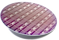
The CCD-in-CMOS technology combines CCD TDI pixels and CMOS readout in one technology, for a low-noise (10 e-), low-power-consumption (<3 W), high-sensitivity, high-speed (up to 300 kHz line rate) chip-scale single-line-scanning imager. Imec developed a single poly CCD pixel inside its 130 nm CMOS imager platform, which includes backside illumination postprocessing. Fabricated on 200 mm wafers, the UV sensor manufacturing steps are also compatible with other postprocessing wafer-level techniques, including spectral filter integration to enable multispectral TDI line-scan imaging. While this latest imager is UV-sensitive, visible-wavelength-sensitive image sensors are also available. Reference: https://goo.gl/qZZLxs.About the Author

Gail Overton
Senior Editor (2004-2020)
Gail has more than 30 years of engineering, marketing, product management, and editorial experience in the photonics and optical communications industry. Before joining the staff at Laser Focus World in 2004, she held many product management and product marketing roles in the fiber-optics industry, most notably at Hughes (El Segundo, CA), GTE Labs (Waltham, MA), Corning (Corning, NY), Photon Kinetics (Beaverton, OR), and Newport Corporation (Irvine, CA). During her marketing career, Gail published articles in WDM Solutions and Sensors magazine and traveled internationally to conduct product and sales training. Gail received her BS degree in physics, with an emphasis in optics, from San Diego State University in San Diego, CA in May 1986.
