Ray-tracing software guides biosensor integration effort
The virtual explosion in the development of optoelectronic technologies during the last 10 to 15 years, particularly for telecommunication applications is providing unique opportunities for other application areas. Researchers at Stanford University (Palo Alto, CA) are leveraging several of these advances in component dimensions and capabilities to develop integrated biological sensing chips. And ray-tracing software is playing a key role throughout the design process.
The researchers are focusing on fluorescence sensing using infrared dyes, partially because of the compatibility of fluorescence sensing with standard biochemical reactions and wide use in the biotechnology community. Another reason, however, is compatibility between infrared-fluorescent dyes and the abundance of high-performance, near-infrared, semiconductor source technology originally developed with telecommunications applications in mind. The latter actually presents a mixed blessing, according to Evan Thrush, a graduate student who presented results from his research team led by Prof. Steve Harris at the annual meeting of the Stanford Photonics Research Center in September.
Potential application areas range from bio-warfare to clinical medicine and biological experimentation with the idea of providing portable and relatively rugged instruments that can take samples and perform elementary analyses, without the need for highly sterile laboratory environments or processing.
"That's where the infrared diagnostic gives you an advantage," he said. "You wouldn't need to get a blood sample taken in the field into its purest form because the blood sample does not scatter as much in the infrared. And what's nice about making fluorescent sensors is that you can make them for any number of applications, capillary array electrofluoresis, as well as in vivo applications."
Myriad of architectures
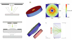
The monolithic integrated sensors being developed at Stanford consist of vertical-cavity surface-emitting lasers (VCSELs), PIN photodetectors, and emission filters arranged in a myriad of potential architectures. Initial software simulations have focused on modeling the fluorescence distribution at the photodetector in proximity and imaging architectures (see figure). In the proximity configuration, the sample is placed close enough to the light source that the light beam from the source is propagated to the biological sample, which then emits photons in all directions. A relatively large, annular-shaped detector is required to detect a significant fraction of the photons emitted from the sample. In various imaging configurations, lenses are used to focus light returning from the biological sample, allowing the use of a much smaller detector. For instance, inner and outer diameters for the proximity architecture detector were set at 100 µm and 1 mm, respectively, while the outer detector diameter in the imaging architecture was only 400 µm.
Simulations done with ASAP compare proximity architecture (top) and refractive microlens imaging architecture (bottom). In both architectures, the downward arrows in the schematic drawings at left indicate light propagation from a VCSEL light source, surrounded by an annular detector. Intervening lens elements direct light in both directions in imaging architecture (bottom). The center images in both architectures simulate an annular detector surrounding the VCSEL. The rightmost images simulate the intensity profile of dye emission at the detector surface (top) and ray tracing of the emitted fluorescence light (bottom).
"There are a lot of pros and cons to the various architectures," Thrush said. Proximity detectors offer relative simplicity of fabrication and relatively large numerical apertures, but are more susceptible to background noise, dark current, and crosstalk. On the other hand, relatively small imaging detectors offer potentially more cost-effective integration and reduction of crosstalk sensitivity. But numerical apertures are normally limited to less than 0.2, while fabrication technologies are likely to be more complex.
In a proximity architecture simulation using ASAP (Breault Research Organization; Tucson, AZ), a "biological sample" containing 5000 IR800 (LI-COR; Lincoln, NE) molecules was located on a slide 0.5 mm from the sensor surface and illuminated by a 780-nm laser diode at 1 mW. A fluorescence collection efficiency of 47% was achieved, with only 5 nW of directly reflected laser radiation incident on the detector surface, indicating that significant spatial filtration may be possible in the proximity configuration.
Future challenges
A pressing demand for the ray-tracing software will be in modeling lateral transmission of the laser beam, which is located in the center of the annular detector. "Even though you have a laser, it doesn't only emit photons in the vertical beam direction. It's also emitting photons out of the side, and one of my big worries is that a fraction of those photons are going to be collected at the detector," he said. "We have a filter on top of the detector to block the laser emission that comes from the top, but the filter will not be able to block laser emission that comes from the side."
Another significant challenge lies in modeling scattering of the laser signal due to specular reflections at various surfaces in the detector system. With laser intensity nine orders of magnitude above the desired detector sensitivity, even relatively miniscule lateral emissions and specular reflections would basically cripple the device, so modeling that parameter is expected to provide the data necessary for design strategies such as placement of optical isolation layers.

