InGaAs detectors allow ultrafast data transfer
InGaAs detectors allow ultrafast data transfer
Photodiodes are critical elements in 1.3-µm high-speed optical
data-transmission systems for
telecommunications, data
communications, and cable
television.
Jay Liebowitz, Krishna Linga, Jim Rue,
Joe Calvitti, and Nitish Agrawal
The communications industry`s need to transmit increasing amounts of information has spurred the fiberoptics community to develop economical, high-speed transmission techniques. Production of components for such systems, such as low-cost 1.3-µm detectors operating at digital rates between
600 Mbit/s and 2.5 Gbit/s and analog speeds approaching 1 GHz, presents challenges in device structure, optical coupling, and package design.
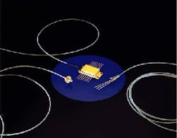
The indium gallium arsenide (InGaAs) positive-intrinsic-negative (PIN) photodiode is the most widely used detector in 1.3-µm transmission systems (see Fig. 1). Primary applications for these devices are data communications (datacom) and telecommunications (telecom). In datacom,
125-Mbit/s fiber distributed-data interface (FDDI) and 200-Mbit/s Enterprise System Communications Network (ESCON) constitute the major uses, though asynchronous transfer mode (ATM) is expected to require comparable volumes in the near future. In telecom, three receiver applications account for nearly all the consumption: 1.5- to 140-Mbit/s asynchronous feeder networks, 155-Mbit/s synchronous optical network/synchronous digital hierarchies (Sonet/SDH), and 20-52-Mbit/s fiber in the loop.
There are a number of reasons why InGaAs PIN photodiodes are the most commonly used detectors. InGaAs provides high responsivity, typically 0.9 A/W at 1.3 µm, and the material contributes only small errors to the measurement of the received optical signal (see Fig. 2). Responsivity stays constant to optical input power levels greater than 1 mW. In addition, the dark current of a well-designed 75-µm active diameter InGaAs PIN photodiode is inconsequential compared to the sensitivity of a 155-Mbit/s fiberoptic receiver. Device costs are low, due to high semiconductor fabrication yields and relatively mature, and now straightforward, packaging techniques. Finally, InGaAs PIN photodiodes are easy to interface with a typical receiver circuit, operating readily from a 5-V supply. For these last two reasons, PIN detectors are considerably more appealing to receiver designers than avalanche photodiodes.
Device design and structure
The speed of an InGaAs detector begins with the structure of the diode itself. For applications between 450 and 1800 MHz, the intrinsic speed of an InGaAs PIN photodiode with a photosensitive diameter of <100 µm is sufficient. This bandwidth derives from several parameters. Optimization of these parameters requires performance/production trade-offs.
The capacitance of an InGaAs PIN photodiode decreases as the device diameter is reduced. The smaller the diameter, however, the greater the difficulty of coupling light from an optical fiber into the detector, which can in turn increase packaging cost. It becomes a design trade-off between cost and performance. Typical photosensitive diameters for high-speed applications range between 25 and 75 µm.
Increasing the thickness of the light-collecting active region decreases capacitance. At the same time, this increases a parameter known as transit time (the time required for the carriers generated from the absorption of photons to travel to the charge-collecting regions on each side of the active layer). Transit time becomes a concern when the frequency of the light signal approaches the reciprocal of the transit time. For a 3-µm-thick active layer, this frequency is 6.7 GHz. The device designer seeks to find the minimum cumulative effect of capacitance and transit time, with the added caveat that the thinner the active layer, the fewer photons the diode will absorb.
The device designer tries to minimize doping of the active region. An InGaAs PIN photodiode derives its ability to function as a phototransducer from the way in which the three layers are successively doped from positive to negative polarity across three layers. The lower the doping of the middle, active layer, the lower the capacitance becomes, increasing the speed of the diode. Material improvements have increasingly made the production of lower doped active regions, and so, higher-speed devices, increasingly common and less expensive.
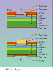
Capacitance from the photodiode electrical bonding pad also influences device design. In the two InGaAs diode configurations, front- and back-illuminated, electrical contact to the n-side is made through the indium phosphide (InP) substrate (see Fig. 3). In the front-illuminated design, light enters through the p-side, necessitating location of the p-side electrical contact outside the active region (see Fig. 4). This contact is a bonding pad, or metal plate, that increases the effective capacitive area acting on the diode junction. Typical bonding pad diameters are between 20 and 30 µm, roughly the same order of magnitude as the diameter of the active region, and can significantly increase the diode capacitance.
Light enters the back-illuminated diode through the n-side, enabling location of the p-side bonding pad immediately over the junction area of the device. This placement keeps the effective area of the junction constant, and capacitance is not increased. Coupling light into the back-illuminated device is slightly more difficult than into the front-illuminated diode, but its lower capacitance significantly improves high-speed performance, as discussed below. The better performance from packaging allows manufacturers to design higher-speed detector modules with the back-illuminated version.
Optical coupling
Optical alignment tolerances, overfilling, and optical return loss are all issues in fiber-to-detector coupling. A high-speed design will almost certainly use a 9/125-µm single-mode fiber. At these speeds, manufacturers typically couple light directly from the fiber into the detector without lenses. The axial distance between the fiber and detector is a minor issue, with tolerances as large as 𫏌 µm. The lateral alignment tolerance, however, is just 䔮 µm. These tolerances are necessary to ensure that none of the light falls outside the active area.
Light reflecting back from the photodiode to the transmitting laser diode can degrade laser performance. To minimize this problem, the photodiode return loss, or back reflection, must be greater than 45 dB. This can be achieved by angling the fiber face nominally 8° from the diode surface. Typically, the manufacturers polish the surface of the fiber to the correct angle finish. Other more-complicated solutions addressing optical coupling and back reflection involve creating a lens on the tip of the fiber.
Developing higher-speed components
Receiver designers are interested in InGaAs PIN photodiodes capable of handling higher transmission rates. The desire for these high-transmission-rate devices is increasing as demand for high-speed systems grows in telecommunications and cable-television (CATV) applications. In telecom, the key rates are 622 Mbit/s, which has an equivalent analog -3-dB point of
415 MHz, and 2.488 Gbit/s, with an equivalent -3-dB point of 1.7 GHz. In CATV, which uses an analog amplitude-modulated (vestigial sideband (AM-VSB) format, the major speeds are 750 and 860 MHz. For PIN photodiodes, telecom transmission distances are up to several kilometers; CATV distances extend as far as 20 km.
Packaging significantly influences the performance of the photodiode in a high-speed receiver. The primary goal of the package designer is to minimize the parasitic capacitance he or she adds to the existing device capacitance. For example, a 75-µm-diameter front-illuminated InGaAs PIN photodiode has a typical capacitance of 0.4 pF at a reverse bias of 5 V; a 25-µm-diameter back-illuminated detector has a capacitance less than 0.1 pF at this voltage. The designer can add an additional 0.2 pF to the diode capacitance by placing the chip on a transistor outline (TO) header. By mounting the detector on a ceramic carrier designed for minimal capacitance, he can keep the addition to as little as
0.05 pF. Assuming a 20-W photodiode series resistance and a 50-W load in both cases, the -3-dB bandwidth for the 75-µm diode on the TO header is 3.8 GHz, while that for the 25-µm chip on ceramic is 15 GHz.
The designer will decide between a TO package and a ceramic carrier based on their differences in capacitance and also on issues such as overall package size and cost. The TO package permits design of compact, inexpensive coaxial modules; the ceramic carrier often requires the use of larger, more expensive dual-in-line modules. These size and cost issues have led package designers to opt for TO packages for current high-volume applications requiring bandwidths up to 400 MHz.
Parasitic inductances often lead package designers to use ceramic carriers for speeds greater than 415 MHz. Inductances come from bonding wires and TO package leads or ceramic traces. These parasitics, which are in series between the diode`s output connection and load, produce response peaking and add phase shift. Such transfer-function effects can decrease system bandwidth and frequency response flatness. On the other hand, the designer can extend the bandwidth of a packaged photodiode by controlling and carefully selecting the values of the series inductances. For example, keeping the total series inductance to less than 1 nH can increase the bandwidth of the package and flatten its frequency response.
Some package inductances are purely detrimental, such as those that occur between the photodiode ground and the ac ground of the receiver circuit. To minimize these effects and optimize device performance, the lengths of bonding wires and traces are kept as short as possible, and special high-speed PC board materials and microstrip traces are used.
The increasing demand for high-speed information transmission over several kilometers provides a growing market for InGaAs PIN photodiodes. Inevitably, these detectors will be required to work at even faster speeds and cost less. Industry scientists are developing monolithic integration methods for the future. In telecom, device scientists are integrating photodiodes and transimpedance amplifiers onto single indium phosphate substrates. For datacom applications, engineers are placing multiple detector pixels on the same substrate and developing ribbon fibers to couple light to the elements. For analog AM CATV applications, receiver-circuit design constraints make integration more difficult. The move toward digital signal transmission, however, suggests that detector manufacturers will eventually provide solutions similar to the telecom optoelectronic integrated-circuit receiver.
To realize the full benefit of these monolithic approaches, detector manufacturers will have to make corresponding improvements and cost reductions in coupling and packaging techniques. Such advances, already being pursued, are dependent upon deeper understanding of electronic, optical, mechanical, and thermal properties of materials. Demand will also have to grow sufficiently to justify industrialization of this development work. When this occurs, InGaAs PIN photodiode manufacturers are confident in their ability to provide a component essential to the realization of economical high-speed broadband networks. n
FIGURE 1. InGaAs PIN photodiodes can be housed in different high-speed packages such as a
3-GHz pigtailed, coaxial module; a 2.5-Gbit/s PINFET receiver in a butterfly package; and a 15-GHz pigtailed detector for laboratory use.
FIGURE 2. Spectral responsivity for the InGaAs PIN photodiode is highest between 1000 and 1600 nm. Responsivity of a bare photodiode is 0.9 A/W at 1300 nm and 1.0 A/W at 1550 nm.
FIGURE 3. InGaAs PIN photodiodes can be mounted on ceramic carriers that have grooves for coupling a fiber to a back-illuminated detector (left) or that carry front-illuminated diodes (right).
FIGURE 4. InGaAs PIN photodiode has two configurations. To¥view shows front-illuminated version, and bottom shows back-illuminated version.
JAY LIEBOWIT¥is director of marketing, KRISHNA LINGA is senior engineer, JIM RUE is senior design engineer, JOE CALVITTI is senior engineer, and NITISH AGRAWAL is product development engineer at EPITAXX Optoelectronic Devices, 7 Graphics Dr., West Trenton, NJ 08628.


