IMAGING DETECTORS: Innovative CMOS circuitry helps detectors resist radiation damage
Scientists at Rochester Institute of Technology (RIT) and the University of Rochester (both Rochester, NY) have been awarded $592,000 from the NASA Planetary Instrument Definition and Development Program to design, build, and test, in collaboration with NASA scientists, an imaging detector specifically for use in harsh extraterrestrial environments.
Goals for the device include smaller size, less power consumption, and more radiation tolerance than technology currently in use. Achievement of these goals will lead to lower mission costs and greater scientific productivity, notes Donald Figer, director of the Rochester Imaging Detector Laboratory (RIDL) at RIT and lead scientist on the project. “But, ultimately, radiation immunity is the focus,” he says.
High-energy particles permeate space and can damage electronics by disrupting sites in the crystal lattice of a semiconductor, Figer explains. Once damaged, the material has a higher dark current and a greater probability of trapping photogenerated charge. Together, these effects reduce the sensitivity of a detector, ultimately limiting mission lifetime. One possible solution would be to add heavy shielding to block radiation, but the resulting costs in weight, and potentially in thermal mass, would be prohibitive.
Figer’s team has set out to develop a new detector design based on a marriage of beneficial qualities from CCD and CMOS detectors. CCD detectors, which are most often used for space missions, offer very low noise, but the desirable noise performance is gradually degraded by radiation damage. While CMOS detectors offer intrinsically higher radiation resistance than CCDs, they start out with a relatively high read noise.
CMOS devices tend to have higher radiation resistance because the photogenerated charge is read out immediately from each pixel, rather than receiving prolonged radiation exposure while clocking across an entire CCD prior to readout. Therefore, the Rochester design uses low-power CMOS circuits arranged in high-density packaging within individual pixels to further enhance radiation resistance.
“The effects of radiation are vastly reduced because of a number of features of our design,” Figer says. “First, we convert charge in a pixel at that pixel, rather than transferring it across thousands of other pixels, as in a CCD. Second, our measurement is purely differential. So a charge hit by radiation can be easily identified as a huge, sudden spike in the signal and removed in real time. Note that in a CCD, once a pixel is hit, its signal for that exposure is worthless. Finally, because our circuit is highly differential, it is not subject to long-term voltage drifts due to radiation damage.”
The researchers achieve CCD-comparable read-out noise by sampling the signal using a sigma-delta analog-to-digital (A/D) circuit with a feedback path that restores charge to the charge-collection node. The new detector is based on a patented technology invented by Zeljko Ignjatovic and colleagues at the University of Rochester, and commercialized through Signal Sciences (Rochester, NY).
So far, the team has fabricated and measured performance in early design prototypes. The researchers expect to ultimately achieve read noise on the order of 0.3 electrons, less than a third of the noise of current CCD technology, and power consumption of 0.88 nW per pixel, three orders of magnitude less than CCDs and more than one order of magnitude less than current CMOS technology.
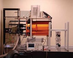
During the course of the three-year project the device will be tested at the RIDL, a new facility established to develop detector technologies for next-generation ground-based and space telescopes (see figure). In addition to Ignjatovic, Figer’s team includes Zoran Ninkov from RIT, Melissa McGrath from NASA Marshall Space Flight Center (Huntsville, AL), and Shouleh Nikzad from NASA Jet Propulsion Laboratory (Pasadena, CA).
About the Author
Hassaun A. Jones-Bey
Senior Editor and Freelance Writer
Hassaun A. Jones-Bey was a senior editor and then freelance writer for Laser Focus World.
