Indium gallium arsenide handles broad task spectrum in near infrared
MARTIN H. ETTENBERG AND
ROBERT M. BRUBAKER
null
Indium gallium arsenide (InGaAs) is the premiere detector material for monitoring and imaging applications in the telecommunications industry. Photo diode arrays of InGaAs also have numerous commercial, industrial, and military applications. The high quantum efficiency of the material in the wavelength range of 0.9 to 1.7 æm and its ability to operate at room temperature make it optimal for detection products and photonics R&D, specifically for monitoring wavelength-division-multiplexing (WDM) networks.
Direct readout arrays
Direct readout arrays are the most basic photodiode array format, in which the InGaAs array is mounted directly on a ceramic without support circuitry. This provides the user with low cost and maximum flexibility in packaging and readout method. The photodiodes are on a common-cathode substrate with each anode wire-bonded to a ceramic fanout trace.
These devices are used in applications that require space savings, offering advantages over individually packaged photodiodes. A photodiode array is desirable for use with arrayed waveguides, because the photodiode array can be packaged close to the outputs of the waveguides.
Direct-readout devices are also provided in a hermetic package with fiber-ribbon inputs. The compact package and ribbon fiber provide a space-saving and fiber-management advantage over individual photodiodes. The fiber coupling allows choice from any input source, not necessarily in any channel or spectral order.
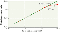
Two key specifications are crosstalk and linearity. The crosstalk of photodiodes on a common cathode will never be better than individually packaged photodiodes, because they are intimately joined both optically and electrically. To minimize crosstalk, a guard structure between the photodiodes removes charge generated outside the photodiodes, which can result from light scattered from the input or from the array itself.
Usually, there is a large incident-light intensity into these types of devices, which makes dark current less important, but pushes linearity to its limit. At large currents, the response saturates due to the series resistance. As the series-resistance voltage drop increases, the diode becomes forward-biased, resulting in a lower output current. The larger the reverse bias applied to the diode, the higher the power that can be incident for a linear output (see Fig. 1).
Multiplexed linear arrays
Multiplexed linear arrays are one-dimensional InGaAs photodiode arrays that are useful for spectroscopy and scanning applications. They are designed to have 100% fill factor so they are capable of detecting light on and between pixels. The photodiode array is hybridized to a silicon complementary metal oxide semiconductor (CMOS) readout integrated circuit (ROIC).
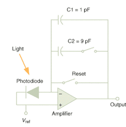
The ROIC typically has a capacitive transimpedance amplifier (CTIA) for each pixel, which simultaneously integrates charge over a given exposure time for all the pixels, and a multiplexer to output the voltage from each pixel serially. The charge includes the signal from photons and dark current from the detector. The CTIA is chosen for near-zero-bias operation and linearity over a large dynamic range. Zero bias is needed to keep the dark current small (a few picoamps) relative to the photocurrent (1 æA maximum). The gain and the full-well capacity (how many electrons can be stored) of the devices are determined by the size of the feedback capacitor, the largest of which is typically 10 to 16 pF and is used for telecommunications applications with high power. For applications that are light-starved, such as scientific spectroscopy, the smallest integration capacitor of less than 1 pF is used (see Fig. 2).
Since their inception, a major application for these arrays has been spectroscopy. Monitoring optical networks is a specialized application of spectroscopy to the light in a fiber. An optical performance monitor (OPM) typically consists of a linear array and a spectral- dispersion element, which distributes a continuous spectrum across the linear array. When the transfer efficiency of the dispersion element is known, the OPM operates as a radiometric spectrometer that measures both the spectroscopic and absolute-power characteristics of the light source. The resolution of the system is determined by the number of pixels in the array, the spacing of the pixels, and the optical dispersion of the grating.
There are many reasons why a photodiode-array-based spectrometer is advantageous compared to other techniques, such as a tunable Fabry-Perot interferometer or a rotating-grating spectrometer. The photodiode-array spectrometer has no moving parts, so there are fewer long-term reliability issues. In addition, the photodiode arrays do not require embedded wavelength-calibration sources, nor do they suffer from thermal instability. The arrays also run at much higher speeds than the other techniques.
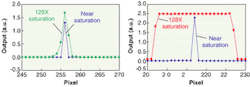
One factor against a linear array compared to a Fabry-Perot or rotating-grating spectrometer is the dynamic range of one acquisition. These devices have one detector with a large dynamic range, and can be adjusted between acquisitions of different wavelengths. So in one acquisition of the linear array, all elements have the same dynamic range simultaneously. A technique to increase the intrascenic dynamic range in a photodiode array is to take multiple images with increasing oversaturation of the peaks.1 This enables detection to a much lower signal level. To accomplish this technique, the detector must have good antiblooming. Blooming occurs when charge from a saturated pixel spills over into adjacent pixels. In hybridized CMOS devices this can be due to saturation of the ROIC input stage, which forces the photodiode current to flow to the neighboring photodiode (see Fig. 3).
Multiplexed area arrays
In the near-infrared wavelength band, area arrays are primarily used in cameras for imaging applications. The cameras include video-rate output either to an analog monitor for stand-alone use by a technician, or to a framegrabber in a computer for quantitative measurements or machine-vision applications. As with the multiplexed linear arrays, the photodiode array is hybridized to a CMOS ROIC. Due to the number and geometry of the pixels, the hybridization method is indium bump bonding, which results in backside illumination of the photodiodes with 100% fill factor.
The ROIC is an "active-pixel" device with an amplifier and storage capacitor in each pixel, and row and column switches to the output amplifier for readout.2 Small pixel sizes ranging from 60 down to 25 æm require the amplifier and capacitor to be carefully chosen. Because of one unrestricted dimension in linear arrays, a large area of the readout may be devoted to storage capacitance. This is not true in the two-dimensional arrays, so different amplifier types are used, such as gate-modulated, direct-injection, and capacitive-transimpedance amplifiers.3 This area limitation leads to smaller full-well capacity and thus restricts the length of integration times from the detector. These devices are primarily used in imaging applications that require a television. For video-rate imaging with a television, 30 Hz is all that is necessary. At 60 Hz the maximum integration time is approximately 16 ms. At this speed, it is also relatively simple to digitize the data for a framegrabber to 12- to 14-bit accuracy. This is typically done to make correcting the image simple so it can be performed in real time onboard the camera.
The camera is used primarily for fiberoptic manufacturing and R&D. The large number of pixels-76,800 for a 320 × 240 and 307,200 for a 640 × 480-make the camera more advantageous for imaging applications than for monitoring the network directly. For monitoring, one needs many scans quickly and the light is generally confined after it has been through a grating. Monitoring with a two-dimensional array requires the system to use a large amount of resources to analyze many pixels, most of which may not have information.
REFERENCES
- Y. Talmi and R. W. Simpson, Appl. Opt. 19(9), 1401 (May 1980).
- L. J. Kozlowki and W. F Kosonocky, "Infrared Detector Arrays," Handbook of Optics, McGraw-Hill: New York, 1995.
- L. J. Kozlowski, J. Luo, and A. Tomasini, SPIE 3698 (1999).
MARTIN H. ETTENBERG and ROBERT M. BRUBAKER are research scientists at Sensors Unlimited, 3490 US Route 1, Bldg. 12, Princeton, NJ 08540; e-mail: [email protected].
null
null