Japanwatch
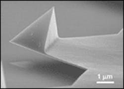
An AFM operates by bringing a small cantilever probe near a sample and detecting the forces between the probe and the sample (see figure). The surface of the sample can be mapped out in this manner. The atomic forces are tiny and highly dependent on the distance between the probe and the sample, so it is necessary to use a microscopic cantilever that vibrates at a high frequency. In this device, a high-frequency laser is used to measure the Doppler shift, thus enabling the observation of a sample with 100-MHz microvibrations.
In the device, light is piped by an optical fiber into a vacuum chamber and passed through a collimating lens, waveplate, and focusing lens before hitting the nanocantilever. The laser light undergoes a Doppler shift depending on the velocity of the cantilever, and returns through the same optical system to be mixed with the control beam. A 1.1-GHz carrier is used, and the frequency shift is detected as a velocity signal. In addition, after the velocity signal of the Doppler measurement is digitized and phase-shifted, the cantilever undergoes self-excited oscillations resulting from an excitation piezoelectric element connected to the cantilever.
The higher the frequency of the target, the larger the Doppler shift. In addition, focusing the laser light, as in this case, does not reduce detection sensitivity. This means that Doppler measurement is a good way to detect high frequency microvibrations in very small objects.
Currently, several new techniques are being developed, including simultaneous observation using 1 million silicon cantilevers of 4-μm size, measurement of atom-level masses using a micron-size cantilever oscillating at 100 MHz, and ultralow-temperature super-high-vacuum AFMs. The mass-measurement resolution of this device has already been established at 10-22 g, with further improvements in the shape and material of the cantilever expected to lead to even higher sensitivity.
Courtesy O plus E magazine, Tokyo
Integrated sensor resolves to 10 nmTOKYOEngineers at NTT Electronics have developed an optical sensor that measures position to a resolution of 10 nm. All its optical elements are integrated on a single silicon chip, making the sensor highly compact. Light-diffraction effects are used to obtain position information, so both linear and angular measurements can be made with high accuracy.Conventional optical position sensors require optical and optoelectronic elements such as mirrors, semiconductor lasers, and photodiodes to be created independently. This inevitably leads to an increase in the number of parts, the number of manufacturing steps, and the overall scale of the assembly and mounting procedure. This new sensor has all-passive elements included in waveguides built into the chip, and also integrates the semiconductor laser and photodiode, leading to a much more compact detector.
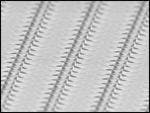
In the device, a waveguide splits light coming from the laser into two beams with a relative phase shift of p/2. The light is guided to a 3.2-μm-pitch diffraction grating attached to the object. The light coming back from the diffraction grating is detected by the photodetector; by analyzing the pattern, the amount of motion can be measured.
The detector also can measure the angular position of an object rotating at very high speeds. By attaching a 3.2-μm diffraction grating to a 12-mm-diameter disk, resolutions as high as 0.00028 degrees were achieved (approximately 1.3 million pulses per rotation).
Because all the optical elements are placed on a hybrid integrated-circuit chip, the device is a very small 1.7 x 2.3 mm. Even with protective materials, the unit is approximately 5 mm on a side. There are few parts and the chip is hermetically sealed, so operation is stable and highly resistant to vibrations.
The detector has many potential uses in compact actuators and manipulators. It can also be used to control the position and orientation of optical-communications components and micromotors, or even in electronic pet robots to achieve more natural movements.
Courtesy O plus E magazine, Tokyo


