Evolutionary design process ponders optoelectronic eye
By Pallab Bhattacharya, Weidong Zhou, Omar Qasaimeh, and Sameer Pradhan
Image sensors for many high-performance applications are based on high-performancebut relatively expensivecharge-coupled devices (CCDs). Moreover, a primary cost factor in CCD-based sensors is the incompatibility between CCD technology and current very-large-scale integration or microelectronic technology.
Therefore, in designing phototransceiver arrays for a proposed adaptive optoelectronic eye as part of a multidisciplinary university research initiative funded by the U.S. Army Research Office, we had to look for an alternative to CCDs for our monolithically integrated image sensors. We decided to develop phototransceiver arrays to provide the optoelectronic parallel processing for our vision systems.
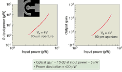
But crucial differences between the demands of high-performance lightwave networks and high-performance vision systems, necessitated a novel design approach for the phototransceiver that has finally yielded a suitable phototransceiver element with a footprint less than 100 μm wide, optical gain of 13 dB, and power dissipation on the order of 400 μW for an input power of 5 μW (see Fig. 1).1
Lightwave vs. imaging
An optoelectronic system basically requires at least three subsystems to simulate the light-detection functions of the human eye. For example, components such as steerable micromachined microlenses, microprism arrays, and the variable focus Fresnel lens (previously demonstrated by our group) would be included in the subsystem of light-collecting optics. Micromechanical components to drive the moving parts would make up a second subsystem, and the third subsystem would include components for image detection, optoelectronic parallel processing, and electronic processing.
The third subsystem essentially requires a densely packed two-dimensional array of photo transceivers that can detect, process, and transmit image signals with a lot of adaptability and efficiency, and is the heart of the optoelectronic vision system. But unlike the requirements of conventional lightwave WDM-based networks, this imaging application has very stringent power-handling and dissipation requirements.
In an image sensor of 100 x 100 elements, for example, the photo transceiver in each pixel should be capable of detecting input power as low as 1 μW or perhaps 0.01 μW. And electrical power consumption in each phototransceiver must also be low, because each pixel in the 100 x 100 array will consist of three to four input colors, and each color will require a separate phototransceiver.
Luckily, some of the requirements for imaging are less stringent than for data communications. Bandwidth is less of a factor because of the massively parallel architecture in the vision system. In fact, the relatively slow image collection speed of the vision system (less than 10 MHz on a focal plane array) is actually limited by the speed of the micromachined optics. System bandwidth can be enhanced in subsequent stages, however, through time-division multiplexing, in which the low-power phototransceivers in the first stage are followed by a second stage of less numerous, high-speed and higher-power phototransceivers of the type used in lightwave networks.
Iterative design process
Actually developing the low-power phototransceivers, however, required an iterative design process. In addition to occupying a relatively small footprint, our phototransceivers would also have to detect relatively low light levels and amplify those signals using only the photocurrent from the detectors to drive the light source. So, for the first step in the design process, we targeted a monolithically integrated device with a 500-μm footprint to match the pixel size of current microlens technology.
In the first iteration, we placed a photodetector and light source side by side. For the photodetector, we used a phototransistor to drive one of two light sources at its output. One light source was a resonant microcavity light-emitting diode (LED); the other was a microcavity vertical-cavity surface-emitting laser (VCSEL). The detector and light source were integrated laterally and grown in one step by molecular-beam epitaxy (MBE). With that design we achieved a phototransceiver gain on the order of 8 to 9 dB with an input power on the order of 1.5 μW, and about 400-μW total power dissipation. At the very low drive currents that we were primarily interested in (below lasing threshold) the microcavity LED provided greater efficiency than the VCSEL.
In the second iteration we attempted to increase the low power sensitivity of the device by replacing the phototransistor with a modulated barrier photodiode, or camel diode, which has the unique property of increasing optical gain with decreases in optical input power (see Fig. 2). In addition, we used a quantum-dot microcavity LED for the light source because of its higher efficiencies compared to normal quantum-well LEDs. These devices, designed and fabricated in collaboration with Dennis Deppe and Diana Huffaker at the University of Texas-Austin, were still integrated laterally and grown in one-step MBE. They boosted optical gain to 18 dB, dropped total power dissipation to just over 100 μW, and were sensitive to input optical powers on the order of 10 nW.
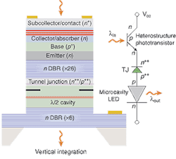
Despite incredible optical performance well in excess of initial design criteria, the footprint of the phototransceiver was still spread over about 200 μm, two times larger than our design criteria. So at that point, we decided to break with conventional wisdom in monolithic optoelectronic integration by integrating the detector and light source vertically instead of laterally (see Fig. 3). The conduit that allowed us to do that was a tunnel junction consisting of a heavily doped p and heavily doped n semiconductor junction that, like an ohmic contact, has very low resistance in both directions of current flow. The vertically integrated device, grown by metal oxide chemical-vapor deposition allowed us to bring the footprint down into the 50- to 100-μm range.
Next steps: phototransceiver arrays
Currently, we've returned to the heterojunction phototransistor, which provides more than sufficient optical gain on the order of 13 dB. The power dissipation is 400 μW, and the input power is about 5 μW. The less than 100-μm footprint allows four phototransceivers to be placed in each 400-μm microlens pixel. Crosstalk on the order of -60 to -80 dB in the arrays was insignificant, and we have demonstrated simple imaging (see Fig. 4).
The next steps for our group involve building slightly denser arrays (we're currently up to about 100 x 100 elements in the lab) and refining our imaging demonstrations. Beyond that, the demonstration of vertical integration using tunnel junctions and quantum-dot light sources opens up new possibilities in far-infrared detectors and focal plane arrays that we have already begun to investigate.
REFERENCE
1. W. Zhou, S. Pradhan, P. Bhattacharya et al. IEEE Phot. Tech. Lett. 13(11) 1218 (Nov. 11, 2001).
ACKNOWLEDGMENTS
Contributors to this work also include Dennis Deppe (University of Texas at Austin), Diana Huffaker (formerly at UT-Austin, now at University of New Mexico; Albuquerque), and Amy Liu (IQE Inc.; Bethlehem, PA).
PALLAB BHATTACHARYA is a professor and SAMEER PRADHAN is a graduate student at the University of Michigan in the Department of Electrical Engineering and Computer Science, University of Michigan, Ann Arbor, MI 48109; e-mail: [email protected]. WEIDONG ZHOU (now at Ciena; Linthicum, MD), and OMAR QASAIMEH (now at University of Jordan; Amman, Jordan) are former University of Michigan graduate students.


