Detector choice is vital to spectroscopy
FRAN ADAR, SALVATORE ATZENI, JOHN R. GILCHRIST, LISA GOLDSTONE, and JON NOONAN
Two main categories of optical detectors are used in analytical instruments: single channel and multichannel. Single-channel detectors have just one element that accepts light through the exit slit of a monochromator. An instrument containing a single-channel detector produces a spectrum by rotating the monochromator grating and recording one data point for each grating position. In contrast, multichannel detectors collect many data points simultaneously without moving a grating or any other part of the spectrograph. This allows much more efficient data collection than for their single-channel counterparts, as large amounts of spectral data can be collected in a single exposure.
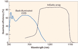
The most popular multichannel detectors are charge-coupled devices (CCDs) made of silicon with several thousand elements, or pixels, arranged in a rectangle. Scientific-grade CCDs exhibit high responsivity from the near-ultraviolet to the near-infrared (NIR) region of the spectrum—200 nm to 1.1 μm. At longer wavelengths, the photon energy is less than the silicon bandgap and the silicon becomes transparent to the incident photons. However, III-V semiconductor materials such as indium gallium arsenide (InGaAs) have a lower bandgap and can absorb the NIR photons (see Fig. 1). For this reason, InGaAs arrays are quickly becoming the array detector of choice between 0.9 and 1.7 μm.
CCD optimized for analytical Raman
Raman spectroscopy requires a very sensitive detector because the signals are usually weak. At the same time, this sort of analytical instrument should be easy to use and should function for long periods with minimal maintenance. Analytical Raman spectroscopy today makes use of compact and reliable lasers, single spectrographs, advanced software, and air-cooled silicon-based CCD detectors. These detectors are usable with most visible-wavelength lasers in order to cover the entire Raman spectral range of interest.
At long wavelengths—perhaps above 750 nm—the quantum efficiency (QE) of these CCDs drops. Modifications are made to the gate structure in order to improve the detection and raise the effective QE. Thinning the polysilicon gate improves response in the middle of the visible range. Applying an ultraviolet (UV) fluorescent phosphor to the surface can enhance the UV response. Excitation of the phosphor with UV Raman photons produces emission in the green that is recorded efficiently by the CCD.
Other techniques improve sensitivity
In a back-thinned device, illumination from the rear of the CCD chip eliminates the problem of absorption from the polysilicon gates on the front. Because the resulting film thickness is comparable to the wavelength of light being detected, however, constructive and destructive interference may occur, resulting in an etalon effect that produces artifacts in the signals, which changes sensitivity. This effect distorts the spectra, changes the analytical results, and is difficult to correct mathematically.
In a device containing open polysilicon gates, approximately a third of the gate is removed in the center of the pixel, allowing more light to reach the silicon, which improves detection. Deep depletion can be incorporated, allowing long-wavelength photons to travel further into the silicon before being absorbed and effectively enhancing the QE for the red region of the spectrum.
Because CCDs are used for many applications, new types are appearing all the time. Pixel sizes are decreasing, which improves resolution, but at the same time decreases apparent sensitivity and imposes slower readout times during analysis. Manufacturers of analytical Raman instruments are constantly making tradeoffs in order to supply high sensitivity while maintaining ease of use and low maintenance requirements.
Fast photoluminescence measurements
The photoluminescence technique can provide information about the material bandgap, impurity content, alloy mix, homogeneity, and thickness of epitaxial layers. In conventional photoluminescent systems, a scanning monochromator equipped with a single-element InGaAs detector is used for analyzing the emission from a sample. The drawback of this technique is that a significant amount of time is required to collect a single spectrum. With an InGaAs array detector mounted onto an imaging spectrograph, however, a large amount of spectral information can be collected quickly and simultaneously. Spectra may be easily collected from samples at room temperature excited by a 532-nm-emitting laser with a 1-s integration time. Excellent signal-to-noise ratio may be obtained with these measurements even for a 1-s measurement time.
Other applications of NIR optical spectroscopy using an InGaAs array detector include Raman spectroscopy, singlet oxygen fluorescence monitoring, IR laser-diode characterization, optical-filter characterization, and photoreflectance. The number of applications is growing rapidly as InGaAs NIR arrays make previously difficult applications more feasible. As part of an integrated system including spectrometer and software, InGaAs arrays will become an increasingly important detector option for the infrared spectroscopist and analytical instrument manufacturer.
A high-bandwidth requirement
Fluorescence lifetime measurements offer temporal resolution of spectra, providing a much more detailed observation of the molecular processes that occur in biology and biophysics, materials science, and chemistry than can steady-state measurements alone. The fluorescence lifetime τ of these materials generally ranges from a few picoseconds to hundreds of nanoseconds. The bandwidth requirements of a detector must be considered for such measurements: at first approximation, the value of 1/τ for a 10-ps decay is 1 × 10¹¹ 1/s (100 GHz), which creates a difficult design problem.
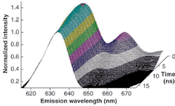
A relatively inexpensive photomultiplier tube (PMT) can be optimized for picosecond lifetime measurements without requiring the use of a microchannel plate or exotic electronics, by careful design of the voltage divider network and radio-frequency construction techniques. At Jobin Yvon, we have optimized a multialkali PMT made by Hamamatsu (Bridgewater, NJ)—a side-on, nine-stage PMT with a wide wavelength response for fluorescence lifetime measurements extending to 10 ps (see Fig. 2). Because the PMT has a risetime of 2.2 ns, one might at first question the notion of using it to measure 10-ps lifetime values. With proper design of the divider circuit, however, it becomes straightforward—at least when the frequency-domain technique of lifetime measurement is used.The theory is simple: a sample is excited with sinusoidally modulated light at a radio frequency (RF), and the resulting emission of that sample is also modulated at the same frequency (generation of such sinusoidally modulated light is usually performed by an electro-optic modulator such as a Pockels cell). The emission signal will lag the excitation signal in phase and be demodulated relative to it; from these two observables one obtains the fluorescence lifetime or lifetimes of the sample. Generally, many frequencies are used over a wide range (10 kHz to greater than 300 MHz) to obtain the frequency-response profile of the sample under investigation.
The reason such short lifetimes can be measured with a 2.2-ns-risetime PMT is the use of the heterodyne technique, in which a second frequency—related to the excitation modulation frequency by a small offset—is electronically mixed with the emission signal by modulating the gain of one of the internal dynodes of the PMT. Thus, the PMT itself is the mixer, and the difference frequency passes down the remainder of the PMT dynode chain where it is amplified, collected at the anode, and passed to electronics for digitization and processing.
Optimization of a PMT voltage divider circuit for this special mode of operation required experimentation to discover the best dynode to modulate (the tradeoff is how much amplification can one achieve before the mixing vs. how high the overall bandwidth of the PMT must be to properly handle the widest possible frequency-response range) as well as RF coupling, termination, and the voltage distribution between the cathode and first dynode and the remaining dynode stages. The entire circuit is kept as small as possible, mounted on a circuit board chosen from a material that offers the best RF performance. Additionally, the implementation can switch the entire voltage-divider characteristics for steady-state photon-counting operation, using control signals from the main instrument-control hardware. With this design, the end user never has to change cables or reconfigure the fluorometer between steady-state and fluorescence-lifetime measurements, eliminating risk of damage to the components while adding full automation of the instrument.
Dynamic range enhancement
Analytical inductively coupled plasma instruments must provide accurate and speedy elemental analysis with full spectral coverage. The detector is required to cover a wide dynamic range at a reasonable cost. Photomultiplier tubes are often used at each wavelength of interest for high speed and stability. However, the dynamic range of the signal may exceed the linear range of the PMT. In this case, the high voltage may be varied to keep the detector in a linear operating mode. The instrument sensitivity is tailored to the measurement of the signal present with automatic hysteresis-free gain adjustment on the millisecond scale. A dynamic range of ten orders of magnitude is maintained. Productivity is enhanced by the measurement of all elements at the concentrations present, both trace and major, in one analysis, usually without the need for a dilution step.
Sensitivity depends not just on QE, but also on the entire optical system, including detector characteristics. The designer of an instrument must also take into account sampling optics, proper dispersive elements, detector coupling optics, low-noise electronics, and processing software to achieve optimum results.
Fran Adar is worldwide Raman applications manager, Raman group; Salvatore Atzeni is principal scientist, fluorescence group; John R. Gilchrist is director, optical spectroscopy division; Lisa Goldstone is worldwide marketing manager, emission group; and Jon Noonan is Internet marketing webmaster at Jobin Yvon Inc., 3880 Park Avenue, Edison, NJ 08820; e-mail: [email protected].

