Sensitive CCDs see the light
by Sheena Devlin
Electron-multiplying charge-coupled devices are the latest imaging sensors on the market. With such a variety of imaging detectors, which sensor is appropriate for which application?
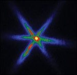
Effective detection at low illumination levels has long been of interest to scientists and has motivated the development and widespread use of highly sensitive detectors. The demand for detection sensitivity continues to increase, however, especially in life science applications (see Fig. 1). Single-molecule measurements, for example, yield very weak emissions and require cameras with enough sensitivity to examine biological interactions in minute samples.
Various kinds of cameras have traditionally been used to detect low light levels: charge-coupled devices (CCDs), intensified CCDs (ICCDs), and electron-bombardment CCDs (EBCCDs). A new species of sensor has recently become available that will push the boundaries of low-light detection even further. The sensor is based on electron-multiplying technology, a novel solid-state sensor design that could revolutionize low-light detection.
Comparing CCD technologies
Charge-coupled devices have several attributes that make them the detector of choice for many scientific imaging and spectroscopy applications. They have the highest and broadest range of quantum efficiencies of any detector available, especially back-illuminated sensors. In general, CCDs have excellent resolution limited only by pixel size, and virtually no crosstalk or other resolution artifacts.
Two such artifacts include "halo" and the "chicken-wire effect." Halo occurs in intensifier tubes when the high-energy electrons incident on the phosphor generate secondary electrons. These secondary electrons are attracted back to the phosphor, creating a halo-like pattern. The chicken-wire effect is a predominant pattern of low transmission lines between multifiber bundles in a fiberoptic used to couple the intensifier tube to the CCD sensor. The lines have a pattern similar to that of chicken wire.
With effective sensor cooling, CCD dark-current effects are negligible. A CCD sensor can achieve low readout noise of 2 to 4 electrons when operated at slow readout speeds. At fast readout speeds, this noise increases. For applications requiring extremely low levels of readout noise, ICCDs or EBCCDs are alternatives.
Intensified CCDs are used most often in low-light applications that require time-resolved measurements of less than 100 μs. Intensified CCDs consist of an intensifier tube positioned over a CCD sensor. The intensifier tube contains a microchannel platea thin disk of honeycombed glass with a high accelerating voltage across it. Photoelectrons generated by incident light cascade down the plate, amplifying the incident signal. This high electron gain effectively results in an ICCD readout noise of less than 1 electron, enabling the detection of single photons. The intensifier tube also provides a means of ultrafast shuttering or "gating" the camera. Optical gate widths down to 2 ns are possible, making it one of the fastest optical shutters available.
In experimental setups, ICCDs are easily synchronized with pulsed light sources. However, the quantum efficiency of ICCDs is much less than that of CCDs because of the photocathode, and even the latest intensifier tubes are only half as efficient as back-illuminated CCDs. The intensifier tube also limits the resolution of the device, and the crosstalk of the microchannel plate has a long, low-level tail. The ICCDs suffer from lag, scintillation, chicken wire, and halo effects, inherent characteristics of intensifier tubes. Their construction is complex and they are more expensive than CCDs.
The electron-bombardment CCD was developed as an alternative to ICCDs. Here, a CCD sensor and a photocathode are positioned inside a vacuum tube. Photoelectrons from the photocathode are accelerated through several thousand volts and are detected directly by the sensor, resulting in a device with a high gain. This provides sensitivity similar to that of ICCDs. No microchannel plates or fiberoptics are situated between the sensor and the photocathode, so EBCCDs have better resolution than ICCDs and do not have to contend with the chicken-wire effect, but do suffer from halo.
Because the CCD sensor in EBCCDs is built into the vacuum tube, the range of sensor formats available for this camera is limited. Overexposure caused by direct detection can damage the CCD, giving EBCCDs a finite lifetime. Electron-bombardment CCDs are complex andexpensive, and, like ICCDs, their quantum efficiency is limited by the photocathode.
Electron multiplication
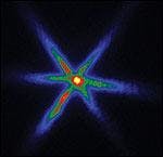
The electron-multiplying CCD (EMCCD) sensor combines the tunable signal amplification typical of an ICCD with the inherent advantages of a CCD, such as high and broad quantum efficiency and high spatial resolution. Also, an all-solid-state construction creates a reliable and robust device. These technological advances have enabled a highly sensitive detector suitable for low-light imaging and spectroscopy applications (see Fig. 2).
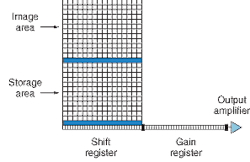
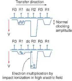
The device achieves this sensitivity by using a unique electron-multiplying structure, or gain register, built onto the silicon (see Fig. 3). The gain register is inserted between the end of the shift register and the output amplifier. Using impact ionization, or the avalanche effect, this structure multiplies the charge packets from each pixel before they are read off the sensor.
The gain register structure is similar to that of the shift register, except that instead of pixels with three electrodes, or phases, per pixel (R1, R2, R3), the gain register has one electrode replaced by two (see Fig. 4). The first of these electrodes, dc, is held at a fixed potential and the second, R2, is clocked as normal, except that a much higher voltage amplitude is used than is necessary for charge transfer alone. The relatively large voltage difference between the two electrodes results in an intense electric field strong enough to cause impact ionization and hence electron multiplication or gain.
The multiplication per charge transfer in EMCCDs is actually quite small, approximately 1.01 to 1.015 times for certain commercial devices.1 When multiplication is executed over a large number of transfers, however, a substantial gain is achieved. For example, using a multiplication per transfer of 1.015 times over a gain register with 591 transfers, a gain of 1.01591, equaling 6630 times, is achieved. Considering that there are no other loss mechanisms, these gain levels mean that EMCCDs exhibit sensitivities every bit as good as and better than the best ICCDs and EBCCDs.2
The output signal from the gain register is fed into a conventional CCD output amplifier with a readout noise of a few electrons root mean square (rms), which increases with readout rate but is independent of signal level. However, as the signal is multiplied by a suitably high gain before reaching the output amplifier, the resultant noise is effectively reduced as it is divided by the gain. This produces insignificant levels of effective noise of less than 1 electron rms at any readout speed.
The gain of the EMCCD sensor is highly dependent on the temperature of the device. A cooler sensor provides greater gain multiplication. Developments in CCD technology have combined EMCCD technology with a maintenance-free hard metal vacuum seal, enabling consistent cooling to temperatures as low as -80°C.
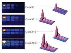
Images of microtitre-plate wells captured with an EMCCD at various gain settings and the corresponding surface-intensity plots provide a direct visualization of electron-multiplying technology (see Fig. 5). In this example, serial dilutions of a luminescent biomarker were placed within the wells of the microtitre plate, similar to those used in high-throughput screening. Images recorded at gain factors of 1x, 9x, 45x, and 500x and the resulting three-dimensional (3-D) surface-intensity plots reveal that the lower concentration wells are indistinguishable from the noise at the unity gain setting. Increasing the gain of the EMCCD makes these wells clearly visible.
Choosing a CCD
With an expanding selection of low-light cameras available, which camera is best suited to which application? In applications that require less than 1 electron of effective readout noise and nanosecond-resolution gating is not necessary (such as single-molecule microscopy, high-throughput-screening techniques, and chemiluminescent detection), an EMCCD camera is ideal. These cameras can be used in any low-light application in which nongated intensified CCDs or back-illuminated CCDs are used.
For imaging applications that require reasonably low readout noise (approximately 2 electrons rms), long exposure times, low dark current, and a wide field of view at high resolution, such as for astronomy applications, a conventional CCD with a large-area format should be used. Intensified CCDs should be used for low-light applications that require fast, gated image capture, such as time-resolved fluorescent microscopy, combustion studies, plasma investigation, and laser-induced breakdown spectroscopy.
REFERENCES
1. D. J. Denvir and C. G. Coates, Photonics West BiOS (Biomedical Optics), San Jose, CA (January 2002).
2. D. J. Denvir and E. Conroy, to be presented at SPIE Annual Meeting 47, Seattle, WA (July 2002).
SHEENA DEVLIN is a technical author at Andor Technology, 9 Millennium Way, Belfast BT12 7AL, Northern Ireland; e-mail: [email protected].