Figure of merit characterizes electronic imager performance
by Chi-Shao S. Lin, Bimal P. Mathur, David L. Standley, and Mau-Chung F. Chang
The large set of detector parameters commonly used to describe performance of electronic imagers can be consolidated into a set of three indices that yield a single figure of merit.
Electronic imaging has become popular in recent years, and this trend will accelerate in the future as electronic camera quality improves while the price falls. Today some digital cameras made with electronic imagers produce quality images that can compete with conventional film cameras. In essence, electronic imagers are beginning to replace film as a medium for image capture. However, user-familiar image-quality indices for electronic imagers are yet to be defined.
Unlike the well-established indices for photographic films, namely modulation transfer function (MTF), ISO speed, granularity, and D-plot, which users can relate to certain image qualities, electronic imagers are usually described by a large set of detector-related parameters and users do not clearly understand the impact of these on picture quality.
Imagers with larger numbers of pixels are considered to offer superior spatial resolution, for example. But in order to increase the pixel number without increasing the chip size, the size of pixel is reduced. Does this imply finer details in the resulting images? A small pixel also means less area for the photogeneration process or a loss of signal strength. In addition, smaller pixels may have higher cross-coupling, so what impact would it have on image quality? Also, how do common parameters like signal-to-noise ratio (SNR), dark current, fill factor, full-well capacity, and sensitivity interact with image quality? Is there any imager performance tradeoff involved among different categories? How can one tell which imager has a better design?
To answer these questions, we first have to establish which performance categories are critical to image quality. Photographic film indices can be roughly divided into three categories: spatial resolution (MTF and granularity), sensing speed (ISO speed and D-Plot), and dynamic range (D-plot).1
It is possible to define a new set of metrics for electronic imagersthe goal is to define one index representing the performance in each of these categories. These new indices are SR (spatial resolution), SP (sensing speed), and DR (dynamic range).
Spatial resolution
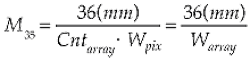
Granularity and MTF are the two most widely used performance indices for photographic films in the spatial-resolution category. The pixel size of an electronic imager directly relates to the granularity index. The pixel size and MTF of an electronic imager, however, cannot serve as a basis for comparison in spatial resolution because the sizes of electronic imagers and lenses used are not standardized. Taking pictures of the same scene at the same field of view with imagers of different sizes requires different reduction ratios between objects and their images.
A normalized MTF will allow direct comparison among imagers of different sizes. Because 35-mm film format (36 x 24 mm) is well-established, it is convenient to use it as the reference size for normalization. The extra image-reduction ratio an imager needs over 35-mm film is given by
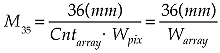
null
where Cntarray and Warray represent the pixel count and the array width, respectively. A 35-mm equivalent MTF, MTF35e of any imager can be defined as:

null
A dimensionless index (SR) can then be defined as the average of MTF35e across a range of spatial frequency (f1) of application interest.
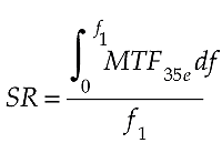
null
Sensing speed
Sensing speed limits the relative motion speed between the camera and objects, and defines the depth of field of the images captured. Some advanced digital cameras have started adopting the popular ISO speed index used to describe sensor "speed." The "ISO speed" of electronic imagers is not well-defined, however. Variable ISO speed is constantly seen because electronic-signal strength changes with different gain factors. We feel that the SNR of the image should be explicitly included or defined when SP related index is being specified.
Kriss has proposed that an electronic imager, which produces an SNR of 30 at 0.8 lux-sec exposure should be defined to have an SP index of unity.2 Adopting this definition to find the SP index of an imager means the value can be obtained by finding the minimum exposure (expressed as a product of light and time of exposureLux · s) required to produce a SNR of 30, and is given by
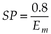
null
Dynamic range
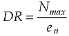
Most electronic imagers respond to exposure linearly, and the noise floor and signal saturation level limit their dynamic ranges. Techniques like logarithmic "compansion" are available to increase the dynamic range of an imager if needed. Linear imagers are very popular, however. For linear imagers, the dynamic range can be measured by an index DR:
null
Nmax is the saturation level and en is the noise floor of the imager, both measured in number of electrons.
Consolidating parameters of electronic imagers
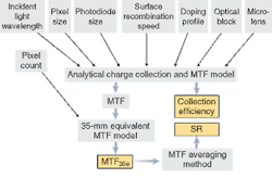
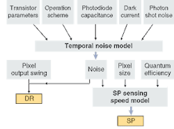
These three critical indices, SR, SP, and DR, consolidate a large group of commonly used engineering terms (see Fig. 1). Parameters including pixel count, pixel size, wavelength of incident light, photodiode size and doping profile, and the use of microlenses and optical isolation, are linked to the spatial resolution index SR.3 Furthermore, parameters including dark current, photon shot and read noise, pixel operation scheme (such as hard or soft reset, correlated double sampling), quantum efficiency, pixel size, output signal swing, and transistor noise are linked to DR and SP indices via the "temporal noise model" (see Fig. 2).4
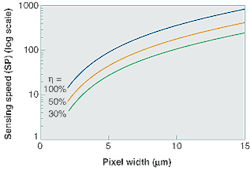
Now the impact on imager performance of engineering parameters can be quantitatively analyzed. The reduction in pixel size from 10 to 5 μm in a particular design, for example, degrades its SR from 0.148 to 0.12. This is because a smaller pixel suffers more from carrier crosstalk. If the imager array size is maintained and the pixel count is doubled, however, SR improves to 0.27. Another simple calculation reveals the limit of the current trend of pixel-size shrinking: an ideal pixel with zero read noise and zero dark current and its noise floor is only limited by the photon shot noise; there exists a maximum SP achievable with a given pixel size (see Fig. 3). If a hand-held camera limits the minimum SP to 100, the pixel size should not be smaller than 5 μm.
Overall performance index
A dimensionless index, can now be defined for imagers, the figure of merit (FoM), which provides an indication of the overall imager performance.5 It is given by
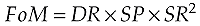
null
The SR index is used in square form because SR relates to quantity per unit length and SP relates to signal generated from a given area in the imaging plane. For an ideal CMOS APS sensor (that is a sensor with no read noise and no cross coupling between pixels), the FoM is given by

null
where k3 is a constant, Vsw is the maximum signal swing, η is the quantum efficiency, Aarray is the imager area, and T is the operating temperature of the sensor. Note that the performance of a CMOS imager is ultimately limited by its signal swing, quantum efficiency of the detector design, and the total imaging area. Performance enhancement in any one of the three indices defined above (spatial resolution, sensing speed, and dynamic range) will imply degradation in the others.
REFERENCES
1. Fujifilm Data Guide, 2000.
2. M. A. Kriss, SPIE - International Society for Optical Engineering, 56 (1998).
3. C. S. Lin, B. Mathur, and M. F. Chang, IEEE Transactions of Electron Devices 49(5) (May 2002).
4. H. Tian, B. Fowler, and A. El Gamal, SPIE - International Society for Optical Engineering, 177 (1999).
5. C. S. Lin, M. F. Chang, B. Mathur, and D. Standley, Proc. International Society for Optical Engineering 4996, Electronic Imaging 2002.
CHI-SHAO S. LIN is an engineer, BIMAL P. MATHUR is president, and DAVID L. STANDLEY is the principal scientist at Biomorphic VLSI Inc., 4165 East Thousand Oaks Blvd., Suite 180, Westlake Village, CA 91362; e-mail: [email protected]. MAU-CHUNG F. CHANG directs the Nanoelectronics Research Facility in the Electrical Engineering Department at the University of California, Los Angeles, CA 90095-1594.