Newsbreaks
Silicon is substrate for gallium nitride-based lasers
At the International Workshop on Nitrides conference (July 22–25; Aachen, Germany), researchers from RWTH Aachen and Aixtron (both of Aachen), as well as the Stepanov Institute of Physics (Minsk, Belarus), presented the first optically pumped gallium nitride-based blue-emitting laser chip fabricated on a silicon (Si) wafer substrate. This is a key result toward achieving low-cost, highly efficient compound semiconductor technologies. The device emits 8 mW of 447-nm light at temperatures up to 420 K and has a lasing threshold of 270 kW/cm2—close to the performance of lasers grown on more-expensive sapphire and silicon carbide (SiC) substrates. The laser was made using Aixtron's metal-organic chemica- vapor deposition process.
Silicon wafers are one-tenth the cost of SiC or sapphire wafers and are also available in much larger diameters of up to 300 mm. Like SiC wafers, they offer high levels of thermal conductivity—particularly important for high-performance electronics—without the insulating properties of sapphire wafers, which can be unfavorable in certain applications. Blue and ultraviolet light-emitting diodes on Si as well as lasers can be produced on Si substrates using this new process.Contact Claus Eherenbeck at [email protected].
Microbolometer has adjustable responsivity
Researchers at the University of Minnesota (Minneapolis, MN) have fabricated microbolometers that have an adjustable thermal conductance, allowing them to be used to measure high-temperature processes such as exothermic reactions. The devices are suitable for forming into arrays. In the design, the detector itself—a thin polysilicon diaphragm—is mounted on support beams over a heat-sink substrate; the diaphragm can be pulled toward the substrate electrostatically, ultimately contacting the substrate. For a low-level infrared signal, the diaphragm position is maintained away from the substrate; the only thermal conductance is through the support beams (the detector operates in a vacuum). For a higher signal, the diaphragm is brought closer to or against the substrate, conducting absorbed heat into the substrate and lowering the detector's responsivity.
In an experiment, the detector's responsivity could be adjusted from 1.20 down to 0.021 V/W (a factor of 50 reduction), while the roll-off .frequency increased from 300 Hz to 9 kHz. It is theoretically possible to change the responsivity by up to five orders of magnitude with this technique. Contact Joseph Talghader at [email protected].
Zirconia waveguides hold up at 2350°C
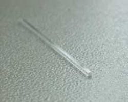
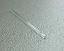
Sapphire optical fibers have been used with great success for high-temperature sensors that provide strain, pressure, and other information. But sapphire softens at 1800°C, preventing its use for some applications. Limin Tong of the Gordon McKay Laboratory at Harvard University (Cambridge, MA) has fabricated rectangular waveguides from single-crystal yttrium oxide-stabilized zirconium oxide (zirconia), which has a melting point of 2600°C. Previous attempts at making sensors from this material concentrated on the fabrication of optical fibers, which had high optical losses.
Tong constructed his waveguides from a single crystal, cutting it into square bars that were then ground and polished to optical quality. The waveguides had cross sections ranging from 0.55 ¥ 0.56 mm to 1.10 ¥ 1.12 mm and lengths to 65 mm. Specimens were tested both in a furnace at 1650°C for 5 h, and in a 2350°C oxyhydrogen flame. Although the flame provided a reactive environment, there was no discernible damage to the waveguides. The average optical loss of the waveguides was 0.016 dB/cm at 900 nm—twenty-five times lower than that for previously made optical fibers of the material. Contact Limin Tong at [email protected].
Meander-type detector counts single photons
In a development with potential for quantum cryptography, researchers at the University of Rochester (Rochester, NY), Moscow State Pedagogical University (Moscow, Russia), and the DLR Institute of Space Sensor Technology (Berlin, Germany) have developed a single-photon detector with counting rates far higher than other techniques such as avalanche photodiodes. The detector's active element is made of superconducting niobium nitride (NbN) and is cooled to 4.2 K.
The detector is constructed in meander-type geometry, where a 0.2-µm-wide NbN stripe snakes back and forth to cover a 4 ¥ 4- or 10 ¥ 10-µm2 area. (Previously, the same researchers had demonstrated a similar superconducting NbN detector, but it consisted of a single submicron stripe, too small to be practical.) Quantum efficiency of the detector ranges from 0.2% at 1.55 µm to 70% at 0.4 µm. The experimental detection efficiency of the larger detector is about 3%, practical for free-space quantum-communication applications. Improvements to the setup will include thinner and narrower meander stripes, a higher meander fill factor, and optimization of the optics that bring photons to the device. Contact Aleksandr Verevkin at [email protected].
Semiconductor laser looks good for twin-photon creation
A room-temperature semiconductor laser fabricated by scientists at Thales Research and Technology (Orsay, France) and the Université Denis Diderot Paris VII (Paris, France) emits in a third-order mode, potentially allowing phase-matching of first- and third-order modes. Such a configuration would allow for the production of twin photons within the laser itself through intracavity parametric fluorescence, in contrast to existing, more-complex schemes in which twin photons are generated in an external nonlinear crystal. The production of twin photons is important for quantum optics and quantum cryptography.
The laser, which is optically pumped with 6-ns pulses from a 532-nm-emitting frequency-doubled Nd:YAG laser, emits at 772.5 nm. The aluminum gallium arsenide heterostructure of the laser contains barriers that force the third-order waveguide mode to have a higher overlap with the single-quantum-well emission region than the first-order (fundamental) mode. The lasing threshold is between 4 and 5 kW/cm2, higher than expected as a result of optical losses. The far field contains the expected three-lobed pattern of the third-order mode (side lobes at ±40°) and fits well with calculations. Contact Vincent Berger at [email protected].
Polymer film may become blue-emitting organic diode laser
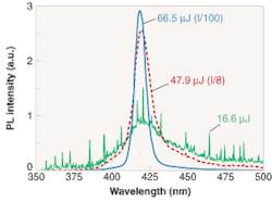
Blue-emitting organic diode lasers may be on the horizon. Researchers at the Universidad de Alicante and the Universidad Miguel Hernández (both of Alicante, Spain) and Washington State University (Pullman, Washington) have observed amplified spontaneous emission (ASE) in optically pumped luminescent polymeric films (red and blue in figure). The appearance of ASE is a strong indicator of lasing ability.
A polymer film such as polystyrene is doped with one or more hole-transporting organic molecules, one example being a diamine derivative termed TPD. The molecules absorb in the 300- to 350-nm range and emit at near 400 nm. Deposited on a substrate with a refractive index of 1.54, the film, with index of near 1.6, becomes a slab waveguide. The film is pumped at normal incidence with 355-nm, 10-ns pulses from a frequency-tripled Nd:YAG laser. As pump intensity increases, the relative emission efficiency increases by a factor of 10; at the same time, spectral narrowing occurs. Lengthening the pump stripe also causes spectral narrowing, furthering the case for ASE. The polymer films have semiconducting properties suitable for the creation of .organic diode lasers. Contact María Díaz-García at [email protected].
Porous gallium phosphide scatters .strongly
Although photonic crystals are grabbing headlines, other photonic materials exist that have their own set of properties. For example, an optical material containing disordered pores on the order of a wavelength or less in size exhibits nonabsorbing scattering properties. Researchers at the Universiteit van Amsterdam (Amsterdam, The Netherlands) and Universiteit Utrecht (Utrecht, The Netherlands) are experimenting with porous gallium phosphide (GaP), a material that is trans.parent from 0.55 to 1.1 µm and shows promise for applications in the visible.
When etched under an electric field, GaP can become porous as a result of electrons tunneling from the valence to the conduction band. The researchers created GaP material with pores on the order of 0.1 µm in diameter in layers with depths of up to 200 µm. Lower dopant densities created larger pores and greater scattering. A transport mean free path of 0.22 µm was measured for one sample, showing it to be the strongest scattering medium of visible light yet found, according to the researchers. A 200-µm-thick layer of the material has a diffuse reflection greater than 99%; introducing an emission source into the pores could lead to strongly scattering random lasers. Contact Ad Lagendijk at [email protected].
Optical receiver tolerates misalignment
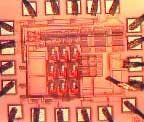
One form of an inexpensive fiberoptic communications link consists of plastic or low-cost glass optical fiber combined with complementary metal-oxide semiconductor (CMOS) optical receivers that can be made in high volume. In this case, the one remaining high-cost system element is the optics used to couple light from the fiber into the tiny CMOS detector (which must be small to reduce detector capacitance and keep bandwidth high). Researchers at IMEC (Leuven, Belgium) have developed an integrated optical receiver that greatly reduces the need for optical alignment of the focused spot on the detector, reducing optics cost.
Rather than one CMOS detector, the receiver contains a detector array, explains Dimitri Linten, one of the researchers (the device shown here has nine detectors and is 150 ¥ 150 µm in size). The spot falls where it may on the device; only the signal from the detector that receives the highest optical power gets coupled to the amplifier. Designed with 0.6-µm design rules, the circuit is optimized for IEEE1394 specifications. Bit-error-rate measurements show that the signal is not degraded by misalignment and defocusing of the incident light beam. Contact Dimitri Linten at [email protected].
Prisms rotate polarization over .large wavelength range
Rotating optical polarization by 90°—required for some interferometric, spectroscopic, and other optical systems—is normally done with a half-wave plate. Ordinary wave plates, however, work over only a very narrow wavelength band; although achromatic wave plates have a larger useful spectral range, they too are limited, especially in the ultraviolet, when they are chromatically corrected only over a range of tens of nanometers. Researchers at Qinetiq (Farnborough, England) and Dstl (Salisbury, England) have developed an optical device that rotates polarization solely by reflection without use of optical coatings, thus ensuring a large achromatic range.
Requiring a rotator that works from 200 to 700 nm, the researchers constructed one out of fused-silica prisms operating in total internal reflection. The design requires three prisms; the surfaces of the spaces between the prisms are oriented at Brewster's angle to reduce loss, while the geometry is designed to compensate for dispersion introduced by the angled surfaces. Seven reflections in a complex three-dimensional path are required for a 90° rotation; the exit beam is collinear with the entrance beam. The .120 ¥ 60 ¥ 60-mm device accepts up to a 20 ¥ 20-mm beam. Contact Roland Appel at [email protected].


