Impact-ionization engineering improves APDs
Impact-ionization engineering and new materials have broadened the range of possible applications for avalanche photodiodes (APDs), while new approaches to avalanche theory are being developed. According to local field-avalanche theory (also known as McIntyre's theory), both the multiplication noise and the gain-bandwidth product of an APD are determined by the ratio of the electron and hole ionization coefficients of the semiconductor in the multiplication region. Impact-ionization engineering (I2E) of APD materials, however, has enabled the fabrication of APDs with noise levels lower than would be predicted by McIntyre's local-field theory. And substitution of new APD materials has allowed significant increases in gain-bandwidth products.
Within the framework of McIntyre's theory, excess noise for an APD material is plotted against gain, and the resulting multiplication noise curve is then used to characterize the material in terms proximate to k values or ratios of ionization coefficients. For instance, silicon has a very low k value (<0.05), which would make it preferable strictly in terms of noise minimization, but indium phosphide, with a k value that is more than an order of magnitude higher than silicon has traditionally been used in APDs for telecommunication applications because of the long-wavelength sensitivity of materials that are lattice-matched to indium phosphide (InP).
Because the ionization ratio essentially represents a material property, for a given electric field, efforts to improve APD performance have traditionally focused on optimizing the electric field profile and characterizing new materials. Recently, it has been shown that aluminum indium arsenide (AlInAs) offers a potential alternative to InP for telecommunications APDs, because AlInAs is lattice matched to InP for long-wavelength sensitivity and also has a k value that is a factor of two smaller than indium phosphide.
Aluminum gallium arsenide with 80% or 90% aluminum, on the other hand, also gives relatively low noise photosensitivity, but because it can't be grown on a substrate that works at long wavelengths, it may eventually prove suitable for applications outside of telecommunications. Recently, however, new parameters have become available for designers seeking to optimize APD performance.
Impact-ionization engineering
"A few years ago we realized that as you begin to shrink the thickness of the multiplication layer the noise goes down," said Joe Campbell, an engineering professor in the Microelectronics Research Center at the University of Texas (Austin, TX). "That was somewhat of a surprise because the theory that we've used for the past three and a half decades predicted the opposite. So we were pleased, but we also had to figure out the fundamental physical mechanisms at play."

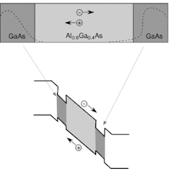
FIGURE 1. An impact-ionization engineered structure has gallium arsenide (GaAs) multiplication layers and an aluminum gallium arsenide (AlGaAs) separation layer (top). The dashed lines qualitatively represent the ionization rates. Electrons passing from the AlGaAs region to GaAs ionize primarily in the GaAs, particularly at low electric fields, and on the other hand, the holes injected into the AlGaAs from GaAs exhibit ionization properties characteristic of AlGaAs, which has lower ionization coefficients than GaAs (bottom). Noise levels comparable to these twin-well structures can also be achieved with single heterojunctions, similar to the one above but without the multiplication region for the holes. The low noise is attributed to single-carrier ionization and spatial localization, but the extent to which acceleration of the electrons in the wide-bandgap layer plays a roll remains an open question.
Delving further led them to a process called impact-ionization engineering, which uses heterojunctions to provide greater localization of impact ionization than can be achieved in spatially uniform structures. The basic idea of I2E is to place thin multiplication layers with relatively low threshold energy on each side of a region with higher ionization coefficients, the separation layer (see Fig. 1).
The purpose of the I2E structure is to enhance impact ionization at the edges in the twin multiplication layers and to suppress it in the center. The central separation layer is used to energize the carriers in transit. Structurally, the I2E device is similar to a truncated multiple-quantum-well APD, but the fundamental operational difference is that I2E does not invoke heterojunction band discontinuities.
"Instead of using just one material uniformly through the multiplication layer, we put in three layers, for example, or perhaps more," Campbell said. "That allows us to localize the multiplication process. And if you localize it, or you tell it where it's going to multiply, it becomes less random and more deterministic. So the statistics are different, and the gain doesn't fluctuate as much."
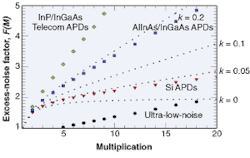
Campbell likened the process to using dynodes in a photomultiplier. "All of the multiplication occurs at discrete points, at the dynodes, and a photomultiplier has very little noise," he said. "It's an imperfect analogy, but some of what we've got to do is make the multiplication process in an APD mimic a photomultiplier." He described the process as a "capricious" one in which "you have to get everything just right." But doing so has provided them with APD multiplication noise levels lower than silicon, the traditional standard for low-noise APDs (see Fig. 2).
A lower limit for scaling down the size of the multiplication regions was presented by the onset of tunneling, and buildup of excessive dark currents. But still, with an I2E APD with two 50-nm-thick multiplication layers and an 85-nm-thick separation region the researchers achieved noise levels corresponding to negative k values for gains less than 20, which presented even more problems in terms of what was at the time, accepted theory.
"When we first saw the low noise, we tried to bend over backwards to figure out how our noise could be low and still fit within the context of the theory," he said. "And in what we published, the experimental work was accurate but our theoretical hypotheses were off the mark. So it took us a while to wean ourselves of this theory, because it had been successful for so long."
They ultimately figured out that McIntyre's local-field theory is based on theoretically predictable ionization taking place across a spatially uniform multiplication region within a uniform electric field. If a significant portion of the multiplication regions consists of "dead space" that allows the carriers to gain sufficient energy to impact ionize, however, the non-local nature of impact ionization can overcome the predicted effects of local-field theory.
"Our colleagues at the University of Sheffield in England have always been strong on the physics of avalanche processes and avalanche photodiodes, and they led the way for us in developing Monte Carlo models and explaining what was going on," Campbell said. "Our Monte Carlo models are coming along now. We've applied them to our newer heterojunction devices, and they are becoming predictive to help us design structures and to say, 'If you do this, you'll see that.' "
Gain-bandwidth products
Incorporating low-noise multiplication regions into resonant-cavity and waveguide structures is also boosting the gain-bandwidth products of APDs into regions that are much more useful for telecom and other applications. "That which gives you low noise also gives you a high-gain-bandwidth product, Campbell said. "So they kind of go hand in hand."
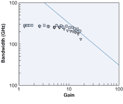
Multiplying the gain of commercially available InP APDs by the 3-dB bandwidth at any point tends to yield gain-bandwidth products lower than 100 GHz, Campbell said. For 40-Gbit telecom applications, an APD with a gain of 10 would require a gain-bandwidth product close to 400 GHz. But a commercially available InP device with a gain-bandwidth product of 90 GHz operating at a gain of 15 would not have sufficient bandwidth to work at 10 Gbits. "You have to back off of the gain to get more bandwidth," he said. "But if you back off of the gain, you have less sensitivity." The ultra-low-noise heterojunction devices, however, are yielding gain-bandwidth products on the order of 320 GHz (see Fig. 3).
Part of the improvement has to do with the heterojunctions to APDs, and additional help comes from applying designs that have already proved successful with PIN photodiodes, such as resonant-cavity and waveguide structures, (see Fig. 4).
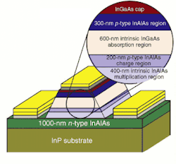
FIGURE 4. Aluminum indium arsenide/indium gallium arsenide (AlInAs/InGaAs) waveguide APD layers were grown by metalorganic vapor phase epitaxy. An n-type indium phosphide (InP) buffer layer was followed by an n-type InAlAs layer. The multiplication layer was grown using doped InAlAs and was followed by an InAlAs charge layer doped with zinc. Two doped InAlGaAs guiding layers bracketed the absorption layer. Finally, a p+ InAlAs layer was topped by a p+ InGaAs cap. To fabricate high-speed devices, a rectangular titanium-platinum-gold p-contact was deposited using a lift-off process.
"The edge-coupled waveguide configuration is attractive for high-speed applications because it permits the absorption region to be thinned in order to reduce carrier transit times without compromising the responsivity, which becomes a function of device length rather than thickness," Campbell said. He added that waveguide devices are also compatible with coplanar interconnects and do not have the wavelength-selective response of the microcavity devices.
While work continues on both heterojunctions and waveguide structures, the capabilities achieved so far are already leading the technology in new directions. One of those is for APD arrays. "Two years ago I would have told you that that is probably not a good idea because small fluctuations in the thickness or doping layers of an APD will change its breakdown and therefore its gain characteristics," Campbell said. But he points to recent work by Larry Coldren's group at University of California, Santa Barbara, which has achieved incredibly uniform 32 × 32 APD arrays. The capability for broad spatial uniformity has also led to requests, beyond telecommunications applications, for large-area APD devices that could be used for imaging.
"Another mode of operation for avalanche devices is to put a DC bias on the detector and then pulse it well above breakdown," Campbell said. "If a single photon comes in during the pulse it can trigger an event, and the APD becomes a Geiger device that can detect single photons."
Such considerations ultimately return to the hoped for congruence between theory and actual results. "The question is whether the things that we've come up with for the other devices, the low-noise and high-gain-bandwidth product, will translate into better single-photon detectors," Campbell said. "And the answer is, we don't know yet."