DETECTORS FOR INTEGRATED PHOTONICS: CMOS silicon-photonic receiver has sub-picojoule-per-bit efficiency
XUEZHE ZHENG, RON HO, THIERRY PINGUET, and ASHOK V. KRISHNAMOORTHY
High-performance digital computing systems continue to be scaled up in speed and capability, most recently in part by increasing the number of processing cores. Further scaling will require not only large interconnection bandwidths with high density, but also ultra-efficient communication links to overcome the difficulties in achieving cost-effective heat removal at both the package and the system level.1 As a result, sub-picojoule/bit communication links are needed for future systems. The unique advantages of silicon (Si) photonic devices suggest photonic interconnects as promising solutions for intra- and interchip applications. However, ultralow-power end-to-end Si-photonic links have yet to be demonstrated.
One of the key building blocks of a low-power photonic link is an energy-efficient optical receiver (see "Previous research on low-power optical receivers" on page 44). A low-power optical receiver requires three key elements: a high-speed photodetector with high responsivity and low parasitics (parasitics are effects such as unintended capacitance or resistance in a circuit design); power-efficient very-large-scale-integration (VLSI) receiver circuits; and integration that has low parasitics.
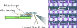
In our efforts to break the picojoule/bit receiver energy-efficiency barrier, we pursued improvements on all three fronts. We used two different platforms to fabricate the waveguide photodetectors and the associated CMOS receiver circuit, mainly due to the different requirements on substrate and other parameters. A custom low-parasitic microsolder technology was used to integrate the photonic device and the CMOS-circuit chip to create a hybrid "CMOS photonic-bridge" configuration with an electrical interface for local communications and optical access for global interconnections via either fiber or waveguides on another chip.
CMOS Ge waveguide photodetector
We developed evanescently coupled germanium (Ge) p-i-n waveguide diodes using single-step low-temperature growth of Ge on Si.5 Grating couplers were integrated with the photodiode waveguides for optical input (see Fig. 1). They were fabricated with Luxtera's Ge-enabled optoelectronic process integrated in Freescale's HIP7 Si-on-insulator 130 nm CMOS node. The Ge detector is very compact, with a size of about 1.5 × 15 μm. Characterization showed that it had a high responsivity of 0.7 A/W at 1550 nm, a low dark current of 3 μA at 25°C, and a 0.5 V reverse bias. At 1 V reverse bias, the detector has an extremely low capacitance of less than 20 fF and a -3 dB bandwidth exceeding 10 GHz. The exceptional quality of the Ge-PIN waveguide detector enabled high-speed receiver designs with high sensitivity.
CMOS VLSI receiver chip
Optical receivers convert a modulated optical signal to an electrical digital signal, using photodetectors as a front end to receive optical signals as photocurrent. Typically a transimpedance amplifier (TIA) converts the photocurrent signal into a voltage, and the voltage signal is then further amplified by multiple limiting amplifiers to a level that can be faithfully identified as either a logical "1" or "0" by the downstream digital circuits. For better energy efficiency, we used a low-power receiver design with a three-stage TIA, followed by a clocked sense amplifier.6 The three-stage TIA gives a total gain of about 1 × 10⁴, producing a 100 mV output voltage for a 10 μA input signal to achieve sufficient signal-to-noise ratio over the transistor mismatch in the sense amplifier and residual thermal noise from both the detector and the circuits. A simple and power-efficient clocked sense amplifier then subsequently amplifies the TIA output to a full-swing CMOS signal. The input referred noise current was calculated to be 1.1 μA.
Conventional optical receivers use analog filter feedback to control and set proper TIA bias, which typically consumes significant power. In addition, it requires DC balanced data, which adds significant energy overhead to the total link power consumption: 25% in the case of 8B/10B DC-balanced coding. To minimize the overhead, we used a digital feedback scheme using a globally synchronized refresh operation to set the TIA bias correctly.6 By periodically refreshing the TIA bias to overcome the signal power variation caused by ambient change and component aging, DC balanced data transmission is not required. The refresh overhead is estimated to be less than 1%.
Low-parasitic hybrid integration
The receiver and detector were then integrated together using low-parasitic microsolder bonding. The fabricated Ge photodetector chip and the VLSI chip were first processed to add under-bump-metallization (UBM) to the bonding pads using electroless plating. Low-profile and small-footprint microsolder bumps were added to the pads on the detector chip after UBM with a few microns of vertical compliance. Two chips were then flip-chip bonded together using thermal compression. The microsolder connections had less than 1 Ω resistance, while the parasitic capacitance due to bonding pads and microsolder bumps was less than 20 fF.
The hybrid chip assembly was die-attached and wire-bonded to a test PCB for power, control, and high-speed digital I/O connections (see Fig. 2).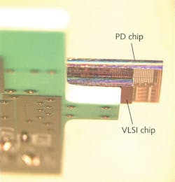
All-CMOS photonic-receiver performance
We tested the integrated receiver performance with a commercial lightwave transmitter driven by 231-1 PRBS data at 5 Gbit/s. A lensed fiber coupled the modulated optical signal to the detectors through grating couplers. The receiver was embedded in a clocked digital link. A high-speed external clock was fed to the chip, aligned with the input data at the sense amplifier, and used to clock the digital data out through the high-speed buffers after the receiver.
With a received optical signal at 18 μA average photocurrent (equivalent to an optical power of -16 dBm for detector responsivity of 0.7 A/W), we obtained error-free operation for more than 6 hr, indicating a bit-error rate (BER) better than 10-14. We further measured the receiver BER for different average input power levels. The result indicates a receiver sensitivity of about -18.9 dBm for a BER of 10-12 (see Fig. 3). We directly measured a record-low total receiver power consumption of 3.45 mW (or 690 fJ/bit) by measuring the supply voltages and currents during operation. This represents the entire power of the photodetector and its CMOS receiver, as well as any excess power required to drive circuit parasitics including internal wiring and flip-chip pads.7 In summary, we have demonstrated the lowest-energy-per-bit optical receiver to date, using a hybrid high-speed Ge photodetector with high responsivity and low parasitics and power-efficient VLSI receiver circuits.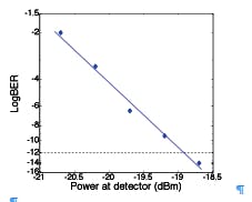
ACKNOWLEDGMENTS
This material is based upon work supported, in part, by DARPA under Agreement No. HR0011-08-09-0001. The authors thank Dr. Jag Shah of DARPA MTO for his inspiration and support of this program. Additional thanks go to Dinesh Patil, Frankie Liu, and Jon Lexau, Sun Labs, Oracle, Menlo Park; Hiren Thacker, Ying Luo, Guoliang Li, Jin Yao, Kannan Raj, and John E. Cunningham, Sun Labs, Oracle, San Diego; and Attila Mekis, Luxtera for their work. The views, opinions, and/or findings contained in this article/presentation are those of the author/presenter and should not be interpreted as representing the official views or policies, either expressed or implied, of the Defense Advanced Research Projects Agency or the Department of Defense. Approved for Public Release. Distribution unlimited.
REFERENCES
1. A.V. Krishnamoorthy et al., Proc. IEEE, 97, 7, 1337-1361 (2009).
2. T.K. Woodward and A.V. Krishnamoorthy, IEEE J. Special Topics in Quant. Electron., 5, 2, 146-156 (1996).
3. T.K. Woodward and A.V. Krishnamoorthy, Electron. Lett., 34, 1252-1253 (1998).
4. D. Guckenberger et al., Proc. IEEE Radio Freq. Int. Circuits Conf., 309-312 (June 2005).
5. G. Masini et al., Proc. LEOS, 848-849 (2007).
6. R. Ho et al., "Circuits for silicon photonics on a 'macrochip,' IEEE Asian Solid-State Circuits Conf. 2009, Industry Session 1-3 (November 2009).
7. X. Zheng et al., Opt. Exp., 18, 1, 204-211 (2010).
Xuezhe Zheng and Ashok V. Krishnamoorthy are at Sun Labs, Oracle, San Diego, CA 92121; and Ron Ho is at Sun Labs, Oracle, Menlo Park, CA 94025; e-mail: [email protected]; labs.oracle.com. Thierry Pinguet is at Luxtera Inc., Carlsbad, CA 92011; www.luxtera.com.