CMOS IMAGERS: sCMOS aims to topple CCD for scientific applications
Choosing a rapid frame rate has traditionally meant compromising on other capabilities such as wide dynamic range. “There are tradeoffs today in imaging detectors,” says Colin Coates of Andor Technology (Belfast, Northern Ireland). You can have one or the other, but not both at the same time. But a years-long collaboration among three commercial vendors—Fairchild Imaging (Milpitas, CA), Andor Technology, and PCO (Kelheim, Germany)—aims to change all that.
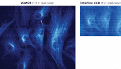
At the biennial Laser, World of Photonics (June 15–18; Munich, Germany), the three companies unveiled the fruits of their effort: “scientific CMOS” (sCMOS). The new technology simultaneously enables up to 100 frames/s and provides inherently low noise (less than 2 e- rms at 30 frames/s; less than 3 e- rms at 100 frames/s) without amplification, wide dynamic range (16,000:1 at 30 frames/s), a quantum efficiency (QE) of 60%, high resolution (6.5 µm pixel size), and a large field of view (5.5 megapixels, 2560 × 2160). In fact, said Fairchild CTO Boyd Fowler, sCMOS will “eventually be a serious contender for the CCD space” in high-end scientific-imaging applications.
Split readout
Key to simultaneously minimizing read noise and maximizing dynamic range is the sensor’s split-read-out scheme, in which the top and bottom halves are read independently. Within each half, every column has a pair of amplifiers as well as two analog-to-digital converters (ADCs). These amplifier/ADC pairs have independent gain settings; the system reconstructs the final image by combining pixel readings from both the high- and low-gain channels. In this way, the system is able to achieve a wide intrascene dynamic range from a very small pixel pitch.
Each pinned-photodiode pixel has five transistors, which enables a number of features including a novel “global shutter” mode. CMOS imagers read out in one of two shutter modes: rolling (wherein lines of the array are exposed as the readout “wave” sweeps across them), and global (wherein all pixels are exposed simultaneously). In sCMOS technology the same sensor offers both read-out modes, allowing the most appropriate mode to be selected for the particular application requirements.
The five-transistor (5T) design also facilitates correlated double sampling (CDS): the sensor’s quantum efficiency benefits from an integrated microlens array, which focuses incident light away from the transistors and onto the exposed silicon (this corresponds to interline CCDs’ use of microlenses to focus light away from the column masks). sCMOS is configured to offer low dark current and extremely low read noise with true CDS. Nonlinearity is less than 1% and correctable to less than 0.2%.
Thanks to the greater than 10,000:1 antiblooming capability (another benefit of its 5T design), pixels can be significantly oversaturated without spilling charge into adjacent pixels, and the sensor or parts it can be held in a state of “reset” even while light is falling on the pixels. The time to transfer charge after exposure completion is less than 1 µs—which makes the sensor useful for fast electronic shuttering and “double-exposure” techniques.
The development partners like to compare sCMOS with interline CCD and electron-multiplying CCD (EMCCD) technologies because both are used in a wide range of scientific-imaging applications. Across most parameters, sCMOS compares favorably—largely without compromise. Still, EMCCD maintains advantages in a couple of areas. For instance, because it is able to multiply the input signal above the read noise floor, it provides a negligible noise level (less than 1 e-). In addition, most current EMCCD cameras provide a back-illuminated format, boosting QE and sensitivity for extreme-low-light applications. But as Fairchild’s Fowler noted, “there’s nothing about [sCMOS] technology that prevents back-illumination” in the future.
About the Author

Barbara Gefvert
Editor-in-Chief, BioOptics World (2008-2020)
Barbara G. Gefvert has been a science and technology editor and writer since 1987, and served as editor in chief on multiple publications, including Sensors magazine for nearly a decade.
