Uncooled infrared arrays sense image scenes
Uncooled infrared arrays sense image scenes
Rapid maturation of microbolometer technology will spur growth and diversification in infrared imaging applications and markets.
Jim Kreider, Phil Howard, Chuan Li, and Tim Fitzgibbons
Cooled infrared (IR) detector arrays were developed decades ago. Like charge-coupled-device (CCD) arrays, they were originally designed for use in demanding aerospace sensing applications. But unlike CCDs, which are now found in everything from consumer products like video cameras to medical and industrial machine-vision systems, the nonmilitary market for IR arrays has never grown beyond small niche applications. Device cost and the complexity of IR sensor implementation have been the major reasons for this lack of widespread use.
This economic picture is now dramatically changing because of a new type of IR array--a microbolometer array--that is silicon based and requires no cooling. Microbolometer arrays differ significantly from conventional IR arrays in terms of performance and applications. The technology is expected to result in cost advantages and a broader range of applications in both the near- and long-term future.
Conventional cooled infrared arrays
Infrared, or thermal, imaging is usually performed in the 8-12-µm or 3-5-µm wavelength region to avoid atmospheric absorption. The longer wavelength band is preferred for applications such as night vision, because an object at 25°C emits roughly 50 times more radiation in the 8-12-µm band than at 3-5 µm.
Until recently, all IR imaging arrays for both these bands were based on photon detection. A photon detector relies on the direct generation of charge carriers (electrons and holes) by infrared photons. This can be accomplished by photoexcitation across the bandgap of a small-bandgap semiconductor material such as mercury cadmium telluride (HgCdTe), by photoexcitation across the metal-semiconductor contact barrier of a Schottky diode such as platinum silicide (PtSi), or by photoexcitation between an impurity defect state and the majority carrier band of an extrinsic semiconductor material such as silicon doped with arsenic (As:Si). With photon detectors, when infrared photons within the appropriate range of wavelengths are absorbed, the photogenerated charge is used to produce a signal proportional to the intensity of the incident IR radiation.
To perform imaging with materials such as HgCdTe or indium antimonide (InSb), detector arrays are fabricated directly onto wafers of the material. Individual detector arrays are diced from the wafers, and the array chips are bonded to complementary metal oxide semiconductor (CMOS) chips that function as readout integrated circuits (ROICs). The ROICs sequentially read out the voltage or charge from each pixel.
Currently, these devices cannot be created monolithically--that is, the array of active pixels and the CMOS structures must be fabricated separately and then bump-bonded or otherwise attached together. A significant thermal coefficient-of-expansion mismatch can exist between the detector array and the silicon ROIC. The mismatch can cause mechanical stresses that limit focal-plane reliability after multiple cool-down cycles. The thermal-mechanical mismatch effect can be reduced by incorporating mismatch compensation structures within the focal plane. These structural requirements make the devices inherently more complex and expensive to produce than CCD arrays, which are all silicon and can be mass-produced monolithically using standard integrated-circuit (IC) fabrication techniques.
At this time, all photon detectors, including monolithic PtSi, require active cooling. The inherent thermal excitation process increases rapidly at higher operating temperatures and thereby competes with the photoelectric process, degrading focal-plane performance by increasing both dark current and noise. These effects are especially significant with the narrow-bandgap semiconductors that are typically used, so photon detector arrays must be cooled. In laboratory applications, a liquid-nitrogen Dewar is often used. In portable radiometers, thermal-imaging cameras, and night-vision systems, a mechanical closed-cycle refrigerator can be used to achieve the required cryogenic operating temperatures. Thus, photon detector focal planes require both complex cryogenic-Dewar packaging and active cryogenic-cooler systems.
Microbolometers instead of cooled arrays
The Focal-Plane Array Team of the Boeing North American (formerly Rockwell) Electro-Optical Center (EOC; Anaheim, CA) has been involved in the design and fabrication of cooled IR arrays for nearly 30 years. For example, the NASA Infrared Imaging Sensor (IRIS) satellite used EOC extrinsic-silicon detector arrays to see newly forming stars and the center of the Milky Way. Also, EOC-produced HgCdTe arrays are currently used in the US space-based early-warning system. Recently, Space Shuttle astronauts integrated EOC-produced 256 ¥ 256 HgCdTe focal planes into the Hubble Space Telescope. EOC is also delivering HgCdTe focal planes to defense customers and PtSi focal planes to commercial OEMs.
As these cryogenic technologies were being refined and matured, it became increasingly evident that the combination of exotic materials, complex focal-plane fabrication and packaging, and the need for active cryogenic cooling would limit IR imaging to relatively high-cost, low-volume applications.
In the early 1990s, researchers at the Honeywell Corp. (Bloomington, MN) developed and demonstrated a completely different type of IR focal-plane array: the microbolometer array (see Laser Focus World, June 1993, p. 101). Several companies, including Boeing North American, have since licensed the microbolometer technology from Honeywell, and they have been developing commercially viable uncooled focal-plane products and imaging engines. To date, however, Boeing is the only one supplying an uncooled microbolometer focal plane--the U3000--on a merchant supplier basis. This technology is offering a lower-cost alternative to cooled arrays and thereby expanding the number of potential applications. We believe that, in the long term, the technology will enable true, high-volume consumer applications.
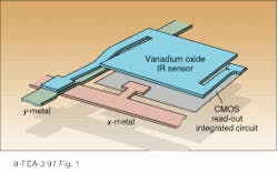
As the name suggests, in this type of array, each pixel consists of a tiny bolometer--a device that measures temperature changes induced by the incident thermal radiation. The temperature is sensed through the strong temperature dependence of the bolometer`s electrical resistance. The bolometer element is a thin-film rectangle of vanadium oxide (VOx) deposited on a dielectric platform supported on two long thin "legs" connecting each pixel to the ROIC (see Fig. 1). This "microbridge" structure represents the fruitful marriage of silicon IC and silicon micromachined-device process technologies. The monolithic wafer fabrication process utilizes standard silicon IC process equipment throughout.
Two key performance parameters are the bolometer temperature coefficient of resistance (TCR) and the pixel irradiant thermal resistance. The TCR is the relative resistance change caused by a 1°C temperature change (that is, TCR = [1/R][DR/DT]).Values of TCR reported in the literature for VOx typically range from 1.5% to 2.5%, with TCRs achieved at EOC typically ~2.5%. The irradiant thermal resistance is defined as the pixel temperature change induced per watt of change in the incident thermal radiation, within the nominal 8-14-µm atmospheric transmission window.
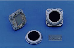
The key design considerations for achieving high irradiant thermal resistance are the pixel thermal absorption efficiency (that is, the percentage of the incident in-band thermal radiation absorbed by the pixel), and the thermal isolation between the pixel and both the ROIC substrate and the focal-plane package environment. Achieving efficient absorption requires careful consideration of the choice of materials, layer thicknesses, and spacings. The average in-band emissivity achieved with the U3000 is typically ~0.8. It is also important to fill as much of the total pixel area as possible with an effective absorbing layer. With the U3000 the fill factor is ~65%. Thus, the U3000`s overall in-band thermal absorption efficiency is ~0.52. Effective thermal isolation is achieved by long thin legs connecting the bolometer to the ROIC substrate and by packaging the focal plane in a miniature vacuum package (see Fig. 2). Typical thermal isolation levels achieved with the vacuum-packaged U3000 focal plane are ~ 8 ¥ 106 °C /W.
The ROIC plays two key roles. First, it provides the planar substrate required for monolithic wafer fabrication of the microbolometer arrays. Second, it provides the critical electrical interface between the 76,800 or more microbolometer pixels and the single-channel multiplexed analog output. It is primarily here that the focal-plane sensitivity, linearity, and dynamic range are determined. Other desirable ROIC attributes are ease of interfacing and operational flexibility. The U3000 is controlled by three external clocks and five biases. The external clocks determine the frame rate and both horizontal and vertical blanking. The focal-plane output signal can be externally controlled to comply with both US and PAL TV synchronization standards.
The miniature vacuum package for the uncooled focal plane also contains a refireable vacuum getter and an operating temperature sensor. The germanium window on the front of the package is antireflection (AR) coated to achieve maximum transmission in the LWIR band (8 to 14 µm). The packaged microbolometer focal planes are very robust. For example, the U3000 in Figure 2 has been subjected to standard mechanical vibration and shock conditions and to both thermal shock and thermal cycling, with no detectable loss in either operability or performance.
Performance
How does the microbolometer array compare to cooled, photon detector arrays? A conceptual comparison is the relation between fast photographic films and slow films. Both film types are fully capable of producing high-quality images. Slow films, however, require longer exposure times and faster optics. This comparison holds equally well for the cooled and uncooled focal-plane technologies. The objective measure of comparison most often used is the NETD (noise equivalent temperature difference). This is the temperature difference that will produce a change in signal equal to the focal-plane readout noise (that is, a signal-to-noise ratio of unity).
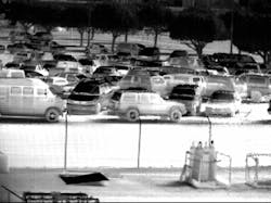
When used with f/1 imaging optics, the current generation of microbolometer arrays exhibits NETDs of ~0.1 K at 30 frames/s; VOx-based microbolometer focal planes will soon achieve NETDs of 0.03 to 0.05 K. Although not quite as sensitive as a cooled PtSi array (typical NETD = 0.05 K) or a cooled HgCdTe or InSb array (typical NETD = 0.025 K), the performance is already more than sufficient for many applications, particularly in surveillance and night vision. For example, the quality of an image obtained using the U3000 in a camera is virtually indistinguishable from the image quality produced by a cooled array under similar viewing conditions (see photo, p. 139). Also, with the uncooled arrays, crosstalk and blooming are never a problem. The microbolometer arrays do not need to store and transfer charge as does a CCD, and the thermal isolation between the pixels is essentially infinite.
In the practical considerations of cost and ease of implementation, there is no comparison between microbolometer technology and traditional cooled arrays. Because the uncooled devices are produced using conventional semiconductor fabrication techniques, they can be economically manufactured in high volume using existing automated fabrication technology. Imagers and cameras using these devices are all-solid-state with no moving parts, such as cryostats or internal choppers. Without cryogenics, the array and stabilizer draw very little power (a nominal 1 W) making this technology ideal for portable, battery-powered applications. Also, because the detector is monolithic, unlike laminated or bump-bonded arrays, it is very rugged with great field stability. It has been exposed to forces exceeding 10,000 g with no adverse effects on performance.
Future development and applications
Clearly, uncooled IR arrays represent a revolution in infrared technology. Two areas in which we expect to see improvements are performance and device integration. Sensitivity should increase severalfold in the near future. For instance, one fairly simple way to increase sensitivity is to adjust the composition of the VOx to increase its TCR value. Doing so, however, makes it more difficult to control material uniformity. This problem is attracting substantial research attention, and development of devices with twice the sensitivity of the U3000 is underway. This will allow higher-sensitivity systems or simpler, lower-cost f/2 optics.
In terms of integration, the uncooled array is following a path similar to that of the CCD and even the CPU chip. As the sensors become more complex and sophisticated, their compatibility with multichip module (MCM) and surface-mount (SM) technologies will be exploited to produce more highly integrated imaging engines. Device manufacturers such as Boeing are already moving in that direction.
Based upon the performance and economics of existing devices, as well as the projected characteristics of next-generation products, uncooled arrays are finding application in night vision, fire-fighting, process control, quality control, robotics, search and rescue, border patrol, vehicle collision-avoidance, security, and medical diagnostics.Their use as helmet-mounted vision aids for firefighters is a particularly exciting application. Limited vision is a major problem in fighting fires, particularly inside buildings; IR detection has the ability to produce clear images through smoke and fog. The use of an IR camera could thus significantly reduce both loss of property and loss of life. Given that more than 100,000 fire helmets are sold annually in the USA alone, this could represent a sizable market.
Another potentially large consumer application is a night/fog vision and/or threat-warning system for automobiles. Such systems have already been installed and demonstrated on futuristic-type vehicles, with the display projected onto the lower part of the windshield. At this early stage, however, predicting the future commercial use of uncooled arrays is akin to electrical engineers prognosticating on the future of the microprocessor, say 20 years ago. As technological advances improve performance and volume production reduces product prices, uncooled infrared arrays can be expected to play an increasingly greater role in the consumer marketplace. o
Uncooled microbolometer sensor provides detailed information about parked cars. This scene was obtained at twilight with a camera containing a U3000 focal-plane array and an f/1 lens.
FIGURE 1. The active sensor that forms each pixel is a vanadium oxide microbolometer. Thin support legs provide electrical contact with thermal isolation.
FIGURE 2. The UM3000 sensor is mounted in a hermetically sealed, evacuated package with a long-wavelength IR filter window.
Jim Kreider is product manager, Phil Howard is senior technologist, Chuan Li is manager of development programs, and Tim Fitzgibbons is senior technical staff on the Uncooled IR Focal Plane Array Team, Boeing North American Inc., Electro-Optical Center, 3370 Miraloma Ave., Anaheim, CA 92803.


