Custom silicon photodiodes offer design flexibility
Yuval Tamari
Photodiodes can be fabricated to meet a wide variety of applications, if you carefully specify your requirements for physical packaging and electro-optical performance. Design choices for photodiodes may differ from those you might make for other types of semiconductors.
The physical part of the electronic design of photosensor devices is inherently simple. A silicon photodiode is a solid-state device—typically a p-n junction—that generates current in direct proportion to the number of photons it absorbs. This response is linear, over a range of seven orders of magnitude. The lower limit of detectability is in the pico watt range, several orders of magnitude less than the human eye can see. The upper limit is the point of irradiation saturation, which occurs at about 1 W/cm2. (For comparison, sunlight at the earth’s surface is about 120 mW/cm2.) Silicon photodiodes respond in the spectral range from 200 to 1100 nm, with peak response at 900 nm.
From the standpoint of electro-optical design, the advantages of silicon photodiodes include this exceptional linearity of output, as well as speed of response. The maximum frequency at which modern photosensors will produce current is somewhere in the 2-GHz range, depending on the type of silicon material used and the size of the detector.
Design flexibility is a major advantage. The output characteristics of a silicon photodiode are determined by the shape of the sensor and the ways in which the sensor can be scanned by the illumination source. For example, scanning a sawtooth-shaped sensor along its length with a narrow beam will produce a pulsed output.
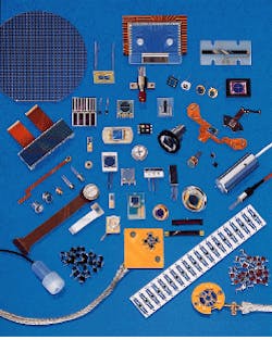
Flexibility extends to the physical packaging options available for photodiodes. Wafer-coating, package-sealing, and chip-fabrication techniques have been developed that make it possible to use silicon photodiodes in harsh environments and to make them either sensitive or resistant to specific types and wavelengths of radiation. Low-cost silicon-wafer fabrication technology makes it practical to produce custom-designed silicon photodiodes in quantity manufactured to exacting specifications, with high reliability and long-term stability of performance, even in harsh environments (see Fig. 1).
This design flexibility has made custom silicon photodiodes the components of choice in such applications as aircraft instrument brightness controls; medical sensing applications such as oximeters, which measure oxygen concentration in the blood of a patient under anesthesia; and glaucoma meters, which measure the opacity of the fluid in the eye. With the addition of a layer of scintillation crystals, detector assemblies can be made sensitive to x-rays. Such detectors are used in computer axial tomography machines, or CAT scanners.
Fabricating photodiodes
As components of electronic design, photodiodes differ fundamentally from other types of semiconductors. Because the purpose of photodiodes is to sense light (or other radiation) from an external source, they are usually mounted off the motherboard and at least partially outside the instrument case. Exposure to light implies exposure to other environmental elements, including dust and moisture. As a result, the design of a semiconductor package becomes crucial to achieving reliable performance under actual operating conditions.
In some designs, the surface of the silicon chip is protected by a thin sheet of glass. Different options are available for sealing the layers of the chip, the glass, and the package, as well as for coating the chip and mounting the package to a printed-circuit board. Thus, even though the electro-optical specifications may be straightforward, the physical packaging of these devices can be quite varied and sophisticated.
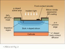
During chip fabrication, the p-n junction, or anode-cathode configuration, of a typical silicon photodiode is formed as layers on a circular wafer, which is then cut into individual chips. Overall, the wafer is about 0.018 in. thick. If the top of a chip is left uncoated, the device is said to be a "naked chip." More often, a coating of silicon dioxide or silicon nitride is applied over the top as protection against moisture and dirt (see Fig. 2).The anode connection can be as small as 0.005 in.2, to which a 0.001-in. aluminum wire is ultrasonically bonded. Because this connection is critical, pure gold plating is required on the printed-circuit board or other substrate to which the device is mounted. Optionally, an antireflection (AR) coating can be applied to the wafer. This coating can be made to either absorb or to reflect specific wavelengths of radiation and therefore to partially control the spectral response of the device. An AR coating also can provide some environmental protection.
Silicon chips are either square or rectangular. Multiple chips are cut from a 4-in.-diameter single wafer, with cuts made at right angles with a diamond saw 0.0015 in. thick. The overall size of each chip, then, can range from 0.020 in.2 to several inches square. Although the square shape of the chip is determined by the fabrication technology, the shape of the sensitive area is entirely up to the designer. This shape is imaged on the wafer by microlithography at a resolution of 1 µm.
Environmental operating conditions will influence the choice of method used to attach the device to either a printed-circuit board or a ceramic substrate. Various adhesives are available to meet temperature conditions ranging from -40°C to 125°C. Case size and configuration, as well as requirements for mounting it, are other important design considerations. Flexible printed-circuit boards may be required when the portion of the instrument that holds the photodiode must permit bending—a flexible wand, for example. Ceramic substrates are often specified if the instrument will be subjected to extremes of temperature.
Electro-optical performance characteristics
An important electrical parameter of silicon photodiodes is silicon bulk resistivity, which can be specified from 1 to 10,000 W-cm. The higher the resistivity, the lower the photodiode internal capacitance. Another design consideration is the diffusion depth of the top layer, which can vary from 200 to 1100 nm. The shallower the layer, the shorter the wavelength (higher the frequency) of the light that can be detected.
If an AR coating is used, its thickness can also be specified to control the response of the device. By varying the thickness of the AR coating, the wavelength to which the device is sensitive can be adjusted by 10% to 20%. Specific wavelengths will be determined mainly by the thickness of the diffusion layer and the characteristics of any AR coating or by the addition of an appropriate optical filter. Filters can be attached directly to the sensitive areas.
For custom silicon photodiodes, these design alternatives do not necessarily have major cost impacts. Tooling costs range from $3000 to $10,000 for a typical lot. The question is not whether a custom chip can be manufactured economically, but whether the choice of design alternatives has been optimized so that the device will perform satisfactorily in its intended application.
YUVAL TAMARI is vice president of Centronic Inc., 2088 Anchor Ct., Newbury Park, CA 91320-1601.

