Solar energy closes in on cost-effective electricity
Advances in manufacturing methods for several photovoltaic (PV) technologies are lowering the cost of making commercial photovoltaic modules. New records in PV cell efficiency are also being reported. Photovoltaic modules themselves must be low-cost relative to the amount of energy they produce. In fact, manufacturing advances have reduced the cost of photovoltaic modules by nearly one third among major US manufacturers, just as many manufacturers in commercial production are scaling up their output (see "Solar market is sunny"; see also "Photovoltaics on the Web"). But laboratory work alone will not lead to cost-effective solar-generated electricity.
There are few global solutions for manufacturing because PV cells can be made in a variety of ways. They can also be made with several types of materials, although all PV cells are basically large-area p-n junction photodiodes (see Laser Focus World, Nov. 1996, p. 137.) This article focuses on common problems in commercial production, as well as manufacturing techniques of each type of cell.
The Photovoltaic Manufacturing Technology Project (PVMaT) is a cost-sharing arrangement between the US government and industry that has been aiding both commercial and precommercial PV companies with manufacturing issues. PVMaT is funded by the Department of Energy and run by the National Renewable Energy Laboratory (NREL; Golden, CO).
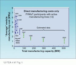
Four of the five major US PV makers are involved with PVMaT, as well as eight smaller manufacturers, says project manager Ed Witt at NREL. The average cost of making a PV module for the manufacturers in the program has been cut by a third to about $3 per peak watt, while the total manufacturing capacity for the companies involved has more than doubled in the last three years. The yearly capacity of a PV factory is measured as the maximum amount of power, Wp, that can be provided from all the modules and cells made during the year. The manufacturers are confident that costs can be reduced further and that the market will continue to grow. By 1999, participants anticipate that they will have average costs of $1.79/Wp and a production capacity increase to 187.4 MW, more than twice the 1996 world capacity (see Fig. 1).Common production problems
Single-crystal silicon wafers are a mature technology and continue to dominate the market, followed by polycrystalline silicon made either by the casting or ribbon-growth method (see Fig. 2). Other commercial PV cells are made from thin films of amorphous silicon or cadmium telluride (CdTe). Some crystalline silicon cells are specialized for use in concentrator modules. Astropower (Newark, DE) straddles the line between bulk and film materials, growing a relatively thick film of polycrystalline silicon on a low-cost substrate.Each wafer material requires a different processing technique, but all kinds of PV modules must minimize the unavoidable costs of materials. Although efficiency for modules in production is always lower than the best individual cells, the drop in efficiency must be contained for all kinds of modules. Encapsulation, which protects the cells from the environment, must be made robust, efficient to apply, and long-lived. Also the formation of electrical connections between the cells and from the cells to a junction box must require little labor.
Materials. "The silicon wafer represents about a third of the cost of a module [for single-crystal and polycrystalline cells]," says Fred Schmid, president of Crystal Systems (Salem, MA). Part of the motivation for thin-film silicon work is its ability to use layers of silicon only a few microns thick, rather than the freestanding silicon wafers that are hundreds of microns thick.
Some cost savings could also be realized if PV makers didn’t need to use semiconductor-grade silicon as a starting material. Semiconductor-grade silicon is not only expensive, it is about 1000 times purer than necessary for photovoltaic use. The lower-grade metallurgical-grade silicon is 99% pure and has about 1000 times too many impurities for PV cells. Recently, says Schmid, there has been a solicitation to produce a solar grade of silicon, which could be cheaper than semiconductor feedstock. Schmid says that the industry needs a supply with volume "into the 100-kiloton-per-year" range that offers lower cost and doesn’t degrade PV efficiency by being too impure. Crystal Systems, which provides furnaces for making cast polycrystalline silicon, has proposed using its furnace technology to produce this grade of silicon.
In addition to the cost of PV material, the cost of the module frame is considerable. A few companies are experimenting with frameless modules. Evergreen Solar (Waltham, MA) is developing a module with a polymer frame that can be heat-formed to the module as part of the encapsulation process. Bill Kanzer of Evergreen says that aluminum frames are the second most expensive element in a module and that the new backskin, which is made of the same material as the polymer frame under development, is thicker and tougher than the popular back-side polymer Tedlar. The prototype polymer frame is lighter and thinner than typical aluminum frames. It includes an aluminum mounting crosspiece on the back. The developers predict that frameless modules could save about $0.50/W from the cost of module making and installation.
Interconnections. Individual cells are connected in series to increase the voltage output. In crystalline cells, conductive tabs attach the contact busbars on top of one cell to the largely metallized bottom of the next. Before this point, each cell is unattached to the rest, so this process requires aligning cells and attaching wires, a complex process. Machinery for aligning and tabbing has partially automated the process, and research is underway to develop a cell geometry that would place all the contacts on one side—this would simplify interconection, making it a planar rather than 3-D process.
Cell interconnections are another production technique in which thin films could gain an advantage over crystalline cells: thin-film cells are formed by scribing apart sections of thin films deposited over large areas—although interconnections must still be made, thin-film cells are already integrated.
Encapsulation. The lifetime of a module depends largely on factors other than the lifetime of the actual cell material. Kanzer comments, "The material will last forever, it`s the metallization and encapsulation [that age]." Metal tabs in crystalline modules eventually oxidize and corrode. The industry-standard encapsulant polymer, ethyl vinyl acetate (EVA), turns yellow and brown under high temperatures and UV exposure. Alternatives to EVA are being researched at NREL, as well as by several PV manufacturers and polymer companies. Ideal encapsulants would be processed like EVA, with comparable costs and optical qualities, but show less yellowing over 20 or 30 years.
Types of crystalline silicon
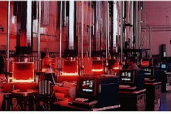
Single-crystal silicon. To make a cell, a boule is grown using the Czochralski method and cut into wafers, then fabricated by forming the junction, applying an AR coating, and adding front (finger and busbar) and back (planar) metal contacts. Because the wafers are round, either the finished modules have a lot of space between wafers or some of the wafer material is wasted by squaring the wafer. An advantage of the Czochralski method, however, is the maturity of the growth process, which is shared with semiconductor-wafer growers.
The largest PV producer in the world is single-crystal silicon manufacturer Siemens Solar Industries (Camarillo, CA). In 1996, Siemens produced nearly 20% of the global output. Ed Witt reports that with support from the PVMaT program, Siemens was able to decrease the cost of its single-crystal silicon module by more than 50% while doubling its US manufacturing capability. Among the improvements were automation and a change in the method of sawing boules into wafers. Wire sawing allows 45 wafers to be produced from a 1-in. section of boule.
Polycrystalline cast silicon. Molten silicon is melted and then allowed to cool slowly (either in the crucible or in a heated mold) into rectangular large-grained semicrystalline ingots before being cut into wafers. This growth method is less exacting than single-crystal growth, and the rectangular wafer shapes solve the packing problem of fitting wafers into the modules without leaving much dead space (see Fig. 3). Manufacturer Solarex (Frederick, MD) automated assembly of the modules (doubling throughput without adding workers), reduced wafer thickness, increased efficiency by changing the cell`s back-surface contacts, and increased ingot size with the help of the PVMaT program.Increasing the ingot size allows more area to be exposed with fewer cuts. Crystal Systems sells automated heat-exchanger-method furnaces for making cast polycrystalline ingots as large as 200 kg (about 450 lb). Fred Schmid notes that multiwire slicing techniques have reduced the amount of material lost during slicing.
Ribbon polycrystalline silicon. Sawing of wafers results in loss of silicon as sawdust. Ribbon growth methods avoid sawing by growing the silicon in thin free-standing ribbons, which are then cut into manageable sizes and fabricated into cells. ASE Americas (Billerica, MA) uses the edge-defined film-fed growth (EFG) method in which a die is pulled from molten silicon in an argon atmosphere (see Fig. 4). The company uses an octogonal die to create a 15-ft-long octogonal tube of multicrystalline silicon with walls about 300 µm thick. The entire tube takes four hours to grow and yields 360 10 × 10-cm cell substrates.Evergreen Solar also produces ribbon polycrystalline silicon, but the ribbon is formed between two high-temperature strings that pass through the molten silicon. Tom Surek, PV program manager at NREL, calls the company’s technology "very exciting."
Film polycrystalline silicon. Another way of avoiding ingot-sawing is to deposit silicon on a substrate. Astropower produces relatively thick films of polycrystalline silicon. Ken Zweibel, NREL’s Thin Films Partnership manager, says this approach provides a low-materials-cost film that adapts known aspects of the material to films. The pilot plant produces a continuous 15-cm-wide sheet of the material on a flexible substrate. Both the polycrystalline growth and n-doping to form the p-n junction are continuous processes. The cell size is not limited by the ingot size as in cast or single-crystal technologies, and the company has demonstrated a single cell that measures 30 × 60 cm, which the company believes to be the world`s largest PV cell.
Thin films
Zweibel says, "Thin films have something to prove." Although developed as cheaper alternative to crystalline silicon, they haven’t been commercially proven. Thin films are put down over large areas, then scribed apart. A transparent oxide conductor can be used as the front-surface contact. Although thin films have been in development for years, they have not been commercialized as quickly as expected due to manufacturing problems. Zweibel adds, "The goal [for thin-film PV modules] is to be competitive in every aspect with crystalline [PV cells]." Surek adds, "On paper, all thin films in large-scale manufacturing look promising." They could even reduce costs to less than $1/W.
Amorphous silicon thin films. With three plants going online in 1997, however, thin-film amorphous silicon has entered the marketplace. These plants alone will produce twice as many modules per year as the total world output of these silicon-hydrogen-alloy cells in 1996. Solarex is ramping up a 10-MW plant in Virginia, Canon has built a 10-MW plant in Japan, and United Solar Systems (Troy, MI) has a 5-MW plant that produces cells on a flexible substrate. Zweibel cautions that manufacturing has just started and hasn’t been optimized yet. Although he doesn’t expect amorphous silicon to dominate the PV market, he does expect improvements in manufacturing over the next 5 to 10 years.
United Solar Systems, a joint venture of Canon and Energy Conversion Devices, is making amorphous silicon modules that can be used as the roofing material. Instead of a glass front, the modules are topped by EVA and Tefzel polymers and backed by a stainless-steel substrate. The manufacturing plant uses a roll-to-roll continuous deposition process that deposits nine layers of film on a 35-cm-wide and 762-m-long substrate. The company has developed a concept design for a 100-MW plant.
Cadmium telluride thin film. PV cells made from an n-doped cadmium sulfide (CdS) layer over a p-doped CdTe layer is a high-risk high-potential technology. Zweibel says, "This technology is the best hope for a breakout—it`s different enough to reduce costs by 50% overnight—if it works." Solar Cells Inc. (Toledo, OH) makes modules that are 9% efficient, and cost is less than $100/m2 now. One of the major challenges is to make the CdS layer uniform while still thin enough to allow light to pass through to the junction. Cell stability and handling of hazardous cadmium are also stumbling blocks. If a reliable manufacturing method is found, costs for these cells could be closer to $1 or $2/W rather than $3 or $4/W, as is the cost of crystalline silicon PV modules.
Photovoltaics manufacturing includes a variety of technologies, among which are many ways that improved or different processes could bring down costs. NREL’s Ed Witt is sanguine about the various paths manufacturers are taking. He says. "There’s a whole lot of right ways to do things."
Solar market is sunny
About two billion people in the world lack electricity, and factors such as democratization, Japanese and German subsidy programs, the drive to electrify rural areas of China, and Worldbank loans are making it increasingly possible for these people to buy photovoltaic modules. In areas without an electric distribution grid already in place, a photovoltaic (PV) module is the simplest solution for providing small amounts of power, says Tom Surek, manager of photovoltaics work at the National Renewable Energy Laboratory (Golden, CO).
The worldwide market for PV is growing rapidly. The editor of industry newsletter PV News, Paul Maycock, says that in 1996 enough cells and modules were shipped to customers to produce 88.6 MW (at peak power), up from 77.6 MW the year before. Surek expects the 1997 market to be about 100 MW.
Despite the high cost of photovoltaics compared to the cost of average utility electricity in the USA, there is a market for electrical service via photovoltaics in some US areas. According to Scott Sklar, executive director of the Solar Energy Industries Association (Washington, DC), about 15% of US customers pay more for electricity than PV costs today.
In the USA, President Bill Clinton announced the One Million Solar Roof plan in June 1997. The plan’s goal is to reduce green-house-gas emissions by equipping one million roofs with PV and heating systems by the year 2010. More than half a million roofs are expected to use PV, which can be estimated to produce 3 GW of output at peak output. This number is particularly astonishing considering that, in 1996, all US PV manufacturers combined produced only enough modules to provide a total of 45 MW. The program is intended to work with green pricing (that is, selling at a premium to people willing to pay more for an environmentally sound choice), low-interest loans, and local tax incentives rather than government subsidies.
The goal isn’t necessarily unreasonable, however. Tom Surek expects that 1997’s world production will be 100 MW and possibly as much as 120 MW. "The companies are limited by production, and prices are going up due to supply and demand," says Surek. Because of demand, he adds, PV module prices haven’t dropped during the last year and a half.
Photovoltaics on the Web
Some very good information on solar energy—both photovoltaic and thermal—is available on the World Wide Web. In addition to Web sites of manufacturers and retailers, the following sites may be helpful for learning more.
NREL (National Renewable Energy Laboratory) Web site contains both technical and basic information about renewable energy resources, as well as information about the US photovoltaics industry.
CREST (Center for Renewable Energy and Sustainable Technology) Web site is less authoritative, but includes a searchable database for different types of information.
PV News, an industry newsletter, has a Web site containing industry information.


