Light emissions from hot electrons have given researchers a new way of testing silicon-based integrated circuits without active probing. The method allows high-speed signals to be tracked as they travel through particular gates and will be usable even as complementary metal oxide semiconductor (CMOS) feature sizes shrink. The technique has already been demonstrated on 0.25-µm devices, and work is underway to perform inspection from the back (substrate) side of a silicon wafer, which would allow chips to be examined despite the presence of many layers of metallization.
Unless they are in transition—when gates are switching—CMOS circuits draw almost no current. During transition, the MOS field-effect transistors (MOSFETs) that make up the gate are saturated for between 10 and 100 ps, creating hot carriers that emit photons through intraband transitions.1 Re searchers Jeffrey Kash and James Tsang of IBM Thomas J. Watson Research Center (Yorktown Heights, NY), have worked on ways of capturing this light. Their goal has been to provide information about how a particular circuit, or a whole chip full of circuits, operates.
The system they use is essentially a microscope with a recording detector. The choice of sensor determines the kind of information that the final image or images will show. The simplest option is the charged-coupled device (CCD), which integrates the low-light signal over time. Images are taken of the silicon wafer as it processes information—exactly what information being determined by the kind of diagnosis required—and the result is a time-averaged picture of the gates that switched. Transistors that were busy during image capture will be bright and the idle ones will be dark. This method could be particularly useful for identifying chips that have faults or making comparisons between identical chips that are behaving differently. It is fast, and an entire chip can be characterized in a single measurement.
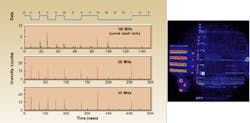
Another option is to use a sensor that can record the incoming photons in time as well as space (see figure). This is not easy because the detector used must have a temporal resolution on the order of tens of picoseconds. The device that the IBM team chose to use is a microchannel plate (MCP) photomultiplier tube (PMT) with a photocathode that can detect wavelengths up to 870 nm. Again, photons were integrated over time to get a usable image, but they were integrated only with photons recorded at the same point in the logic cycle. One way to think of this is simply repeating the same data process many times, capturing a set of time-resolved images for each repetition, and overlaying all of the resulting "movies" on top of each other. Thus, enough photons are counted without losing time information.
In the IBM experiment, oscillating circuits were used that inherently produced an output signal at the end of each loop.2 These triggered the detector, essentially "time-stamping" them. The result, after combining all the recorded data, was a slowed-down motion picture of the electrical signal traveling from gate to gate around the circuit.
Back-side inspection
The next step is to perform this same experiment, but looking at the bottom or substrate-side of the wafer instead of the top. This will be important for real applications because of the increasing use of many metal interconnection layers that prevent light escaping from the silicon. Emissions from the hot carriers produce enough infrared light (for which silicon is transparent) to make this back-side inspection possible. The researchers, however, have come across two major problems—time and wavelength—though in one sense they are both the same problem. Many detectors are sensitive to infrared wavelengths, but none can image a whole plane with enough temporal resolution to make the "real-time" system work. Likewise, the MCP/PMT combination has all the right characteristics except for its inability to see infrared.
If the right image-capture device can be found, the new method should be both powerful and long-lived. Researchers have shown that, as feature sizes decrease, the light emitted per electron through the gate actually increases. Thus, the technique should be even better at diagnosing tomorrow's computer chips than today's.
REFERENCES
1. J. C. Tsang and J. A. Kash, Appl. Phys. Lett. 70(7), 889 (17 Feb. 1997).
2. J. A. Kash and J. C. Tsang, IEEE Electron. Device Lett. 18(7), 330 (July 1997).
About the Author
Sunny Bains
Contributing Editor
Sunny Bains is a contributing editor for Laser Focus World and a technical journalist based in London, England.
