CMOS detectors enable optical interconnects
JEREMY D. SCHAUB
As data rates increase to 5 or 6 Gbit/s, the performance of high-end computer systems is limited less by microprocessor clock speeds and more by the interconnections between microprocessors.
Copper links are limited to less than one meter over traditional (FR4) electrical backplanes and are becoming increasingly difficult to implement at these data rates in the face of power constraints and high aggregate bandwidths.1 Further, these links often require equalization to correct for the significant dispersion of the line. For board-to-board and rack-to-rack interconnects, edge-connector density also limits the system performance.
Incorporating highly parallel optical data links into these systems would enable superior performance in terms of density, power dissipation, and cost, especially for rack-to-rack links with length requirements of 5 to 30 m. Future high-speed backplanes at higher data rates would similarly benefit from an optical solution at even shorter distances.
Traditionally, optical-communication links are designed to operate at wavelengths of 1.3 or 1.55 µm to take advantage of the low dispersion and low attenuation minima of optical fiber. However, at distances of less than 300 m, dispersion and attenuation become less important while larger-diameter multimode fiber with low-cost vertical-cavity surface-emitting-laser (VCSEL) technology, at 0.85 µm, becomes more cost-effective.
For the optical receiver, it would be most attractive to use a silicon photodetector monolithically integrated with a silicon-based complementary metal-oxide semiconductor (CMOS) or BiCMOS amplifier because it leverages the low cost, high reliability, and volume manufacturability of silicon technology. However, the absorption at 0.85 µm is poor in silicon because of the indirect bandgap. The absorption length in silicon is almost 20 µm compared with 1.1 µm for gallium arsenide (GaAs) and 0.27 µm for germanium (Ge). Consequently, it is difficult to design a silicon photodetector with high efficiency in silicon CMOS processes. As a result, optical receivers are traditionally designed using III-V photodetectors, typically with an absorption region of GaAs or indium gallium arsenide (InGaAs), and an amplifier fabricated in silicon CMOS or BiCMOS technology. Using this approach, the photodetector and the amplifier are optimized separately and packaged with wirebonds after fabrication.
This hybrid approach has several drawbacks when designing the highly parallel arrays needed for interconnects in future high-end server systems. First, it is costly and complex to wirebond an array of photodiodes to an array of amplifiers. Second, the high-speed performance declines because of packaging parasitics such as wirebond inductance and bonding-pad capacitance. Wirebond leads also exacerbate electrical crosstalk between channels. One alternative is to use flip-chip technology to attach the chips, eliminating the wirebond step. This approach poses significant manufacturing challenges in terms of alignment and reliability because of thermal mismatch, however, and packaging parasitics continue to degrade performance.
For these reasons, research in the past few years has targeted high-speed silicon-based photodetectors and investigated many ways to demonstrate high-bandwidth silicon photodetectors with reasonable efficiency. Silicon resonant-cavity PIN photodiodes, for example, have been demonstrated with high bandwidth (more than 34 GHz) and good quantum efficiency (42%).2 However, most approaches involve deviating from the standard silicon process flow, rendering the resultant devices incompatible with the CMOS transistors used to design the amplifier. The challenge is to design high-performance devices that require little or no CMOS process modifications.
The traditional photodiode structure is the vertical p-n junction diode separated by an undoped, or intrinsic, absorption region. The intrinsic region increases the efficiency, creates a uniform electric field under reverse bias and reduces the capacitance, which increases the bandwidth. This PIN structure is used extensively for III-V photodiodes because the absorption length is roughly 1 µm. However, the absorption length of silicon is 20 µm, and the vertical PIN structure would have to be many microns thick to attain reasonable quantum efficiency.
This approach has many drawbacks. First, the bandwidth would decrease because it would take a long time for the photocarriers to drift across the absorption region. Second, the operating voltage would have to be high to deplete the absorption region. Most important, the silicon CMOS process involves fabrication steps within a few hundred nanometers of the semiconductor surface. Attempting to incorporate a very thick (much more than 1 µm) PIN structure into this process is simply impractical.
A photodiode structure that is more compatible with CMOS is the lateral PIN structure (see Fig. 1). The design consists of alternating p-type and n-type interdigitated fingers separated by the absorption region, similar to a metal-semiconductor-metal (MSM) photodetector layout. This structure features low capacitance per unit area and, more important, is easier to implement in a CMOS process using the source and drain implants of the n-type and p-type transistors.
In this structure, photocarriers are generated deep below the semiconductor surface because of the long absorption length. These deep carriers drift slowly to the electrodes and can severely limit the bandwidth. Therefore, it is beneficial to block the deep carriers at the expense of quantum efficiency. One method involves placing an insulating layer, such as silicon dioxide, a couple of microns below the surface.3 The thickness of the oxide layer can be adjusted to maximize the reflectivity at the desired wavelength so a portion of light is reflected back through the absorbing region, increasing the efficiency.
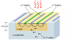
The insulator layer blocks these slow carriers and increases the bandwidth. However, silicon-on-insulator (SOI) substrates are significantly more expensive than bulk silicon substrates, so it is beneficial to realize a similar structure in a bulk CMOS process. An alternate way to block the slow carriers is to use a p-n junction as a screening terminal. The active area is placed inside an n-well surrounded by substrate contacts. Electrodes collect fast electron-hole pairs, generated inside the n-well region, while the potential barrier created by the p-n junction blocks pairs generated below the n-well.
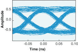
A 30 × 30-µm device with this structure was fabricated in IBM's 0.12-µm foundry process. Open eye operation was obtained up to 4 Gbit/s at a supply voltage of only 2 V. This is the highest reported speed of a silicon photodetector fabricated in an unmodified bulk CMOS process. However, the device exhibited a quantum efficiency of less than 1% at a wavelength of 0.85 µm. This low efficiency is a direct result of the thin absorption region.
An alternate silicon photodiode structure can be formed by modifying the process used to form deep-trench DRAM capacitors (see Fig. 2). The device, named the lateral-trench detector (or LTD), consists of trenches with high-aspect ratios (0.4 µm wide by 8 µm deep) that are formed using reactive-ion etching. The trenches are filled with n-type and p-type polysilicon to create the lateral PIN structure. This extends the absorption length dramatically, compared with the unmodified CMOS device. In addition, the absorption length is decoupled from the carrier transit time. This enables high-speed, efficient operation at low bias voltages.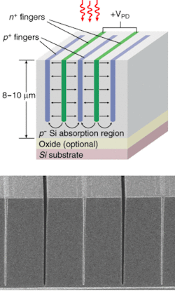
These results demonstrate that high-speed, efficient detectors can be realized using silicon-compatible CMOS processes. There is also much interest in extending to the longer wavelengths used in telecommunications. This would require integrating other semiconductor materials, such as germanium or indium gallium arsenide, with silicon. If successful, this would not only dramatically improve receiver performance but open new packaging approaches because silicon can be used as a waveguide at wavelengths longer than 1.1 µm.
REFERENCES:
- Optical Internetworking Forum (OIF) Common Electrical I/O (CEI) Interface, www.oiforum.com/public/documents/CEIWP.pdf
- J. D. Schaub, R. Li, C. L. Schow, et al., IEEE Photon. Tech. Lett. 11, 1647 (1999).
- M. Ghioni, F. Zappa, V.P. Kesan, et al., IEEE Trans. on Elec. Dev. 43, 7, 1054 (1996).
Jeremy D. Schaub is a research staff member at the IBM T. J. Watson Research Center, 1101 Kitchawan Road, Yorktown Heights, NY 10598; e-mail: [email protected].