Imagers grow to address specialized applications
From x-ray imaging to space telescopes, large-area imagers gain size and sensitivity to meet the demands of these unique markets.
While the world of imagers for consumer-level digital cameras has grown smaller-with devices now available in 0.1-in. formats-the world of large-area imaging is diverse and expanding. Imager size, resolution, sensitivity, and price all play a part as the imaging world leaves film behind. The technology envelope is expanding in all directions and the tradeoffs made today may not apply tomorrow.
Professional photography is transitioning from film to digital media and imager size and resolution have increased to address market need. Kodak (Rochester, New York) and Dalsa (Waterloo, Ontario), for example, are currently offering 22-megapixel color CCD imagers.1, 2 Even larger-area imagers can be used in specialized applications like x-ray imaging (in which the use of lenses is impractical), or under low-light conditions where every photon is precious. Large-area CCDs, fabricated one per wafer, have also found a home in x-ray diffraction applications such as protein crystallography, and-when attached to fiberoptic tapers-in radiography applications that require high resolution.
The largest single CCD imager currently on the market is the 9216 × 9216-pixel CCD595 from Fairchild Imaging (Milpitas, California), which has a diagonal dimension of almost 4.5 in. (11.4 cm).3 And Hamamatsu (Hamamatsu City, Japan) recently introduced a large-area CMOS photodiode array for use in mammography.4 At 11.1-in. (28.2-cm) diagonal active area with a 50-µm-pixel pitch, the device is fabricated entirely on a single 12-in. silicon wafer. The largest of all single-unit imagers now available are amorphous silicon flat panels for medical imaging-with panel sizes up to 17 × 17 in. (43 × 43 cm), they replace film in chest x-ray machines.5
As the available light decreases, design choices like imager size, lens aperture, imager quantum efficiency (QE), read noise, and pixel size become increasingly important. The most sensitive imagers have the highest QE (the percentage of light photons converted to signal electrons) and the lowest effective read noise (the signal electron-equivalent noise). The highest QE is achieved by back-thinning the sensor-a technique in which the image sensor is mounted face down on a support substrate and thinned so that photons can strike the sensor from the back, in the sensitive portion of the pixel, without being absorbed or reflected by the gate structures on the front surface. Back-thinned sensors may have a surface treatment or antireflective (AR) coating applied to optimize the QE at specific wavelengths. For example, 95% of all 550-nm photons may be converted to signal electrons at −20°C with back-illumination and the mid-band AR coating from e2v technologies.6
Silicon-based imagers are sensitive to a much broader spectral range than just the visible band. While medical x-ray imagers use a phosphor coating to convert the greater-than 10-keV x-rays to visible light, it is possible to use silicon imagers for direct detection of lower-energy photons. For the wavelength range from 10 keV (0.12‑nm) to 1.13 eV (1100‑nm), a wide variety of CCD types have been developed for direct photon detection. Back-illuminated CCDs are ideal for the range from soft x-rays to the UV, where the absorption depth of photons in silicon is extremely short. And CCDs built on thick, high-resistivity silicon can capture the wavelength ranges that tend to be absorbed deep in the silicon, especially in the near-IR. Recently, Lawrence Berkeley National Laboratory (Berkeley, CA) developed a CCD with a sensitive thickness of 300 µm. Prototype devices have a QE of more than 90% at 900 nm.7
Noise is important
Quantum efficiency is only part of the story in imager sensitivity. The imager noise level in the absence of light (dark current) also helps set the lower limit on the light detection level. Many techniques have been developed to reduce the amount of charge spontaneously generated in the dark. Dark current from the silicon surface is virtually eliminated by the use of MPP (multiphase pinned) or IMO (inverted-mode operation) operation modes. A state-of-the-art imager will only be sensitive to dark charge generated in the bulk silicon where the signal charge is stored. Dark-charge generation is a function of silicon volume and a larger, deeper pixel will inherently generate more dark charge than a smaller, thinner one. Highly sensitive, large-pixel imagers require cooling to reduce or eliminate dark charge. Once the dark-charge generation is eliminated, the inherent voltage noise in the output amplifier sets the noise floor.
The lowest effective read noise of any imager is available in impact-ionization CCDs from Texas Instruments (Dallas, TX) and e2v technologies.8, 9 An on-chip gain register multiplies signal electrons by as much as 1000 times before they reach the standard CCD output so that the electrons can be seen above the voltage noise. This results in an effective read noise of less than one signal electron, even at video rates. However, the statistical nature of the gain process creates excess noise at higher signal levels, increasing the inherent photon shot noise by a factor of root two. For many low-light situations, a conventional CCD with very long integration times is still the imager of choice. With proper bandwidth limiting, a conventional CCD output can be very quiet at low pixel rates.
The largest imagers
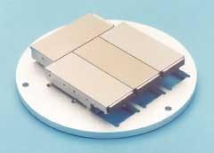
Of all the imaging applications, astronomy has long been the one to drive the market for large-area, highly sensitive devices. Optics on larger survey telescopes can bring to focus an area much larger than a single silicon wafer at a resolution only limited by atmospheric turbulence. To address this market, three-side buttable, large-area CCDs and packages were invented in the 1990s. Buttable packages and devices allow large, extremely flat focal-plane arrays to be constructed. Of course, high QE and low read noise are also required for the image sensors.
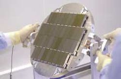
One of the largest focal-plane arrays in the world today is the MegaCam on the 3.6-m Canada-France-Hawaii Telescope atop Mauna Kea in Hawaii (see Fig. 1).10 It has a one-square-degree field of view, approximately the size of four full moons. The array consists of 40 back-illuminated CCDs tiled as closely as possible in a 4 × 9 mosaic with two additional imagers on each side. Each CCD contains 2048 × 4608 13.5-µm pixels with a median peak-to-valley flatness of less than 6 µm. One of the project requirements was that each CCD and package be as similar as possible to allow for future replacement. To that end, the devices were provided in Invar packages with height shimmed to 14.001 mm at a standard deviation of less than 6‑µm. The overall peak-to-valley flatness of the mosaic has been measured to be ±16 µm at operating temperature, much better than the design requirement.
For the MegaCam project the seam between imagers was adjusted to be as small as possible. In the assembly the inactive area between adjacent sensors is 1.1‑mm on the sides and 0.9‑mm at the tops of the imagers. Between the top of an imager and the connector side of its neighbor, the gap is less than 5 mm. The focal plane measures 12.3 × 10.3 in. (313 × 261 mm) with a 93% fill factor.
The MegaCam electronics were designed and built by the French government agency, DAPNIA. The camera is capable of reading out a full image (700 Mbyte) in 20 seconds. It will be used 15 to 18 days per month around the new moon and is capable of taking up to 150 exposures per night (see Fig. 2). Almost 50 terabytes of image data will have to be processed and archived over the next five years.
While MegaCam is possibly the world’s largest focal-plane array today, other larger arrays are under construction. The Large Sky-Area Multi Object Spectroscopic Telescope (LAMOST)-a Chinese Academy of Science project-will have a full 5° × 5° field of view over 1.75 m. The focal-plane array will use 36 CCDs from e2v technologies. With 4096 × 4096 12-µm pixels, each device will be almost twice the size of those delivered for MegaCam. The telescope will be used to take a spectral survey of the sky, providing spectral data to accompany the imaging data available from other sky survey telescopes (see Fig. 3).
The use of focal-plane arrays is not confined to Earth; there are many in space now and planned for future space missions. The European Space Agency is developing hardware for the Gaia mission to make a three-dimensional map of the Milky Way galaxy. e2v technologies will supply 180 custom CCDs to be used in the focal-plane array, which will be used in time-domain-integration (TDI) mode in which the image is scanned across the array while the signal in the imagers is synchronously transferred under it. The imager’s pixel size will be 10 µm in the scan direction and 30 µm perpendicular to it, while the pixel count will vary, depending on location in the array. The overall focal plane is planned to be 30.2 × 23.6 in. (768 × 600 mm).
Large-area imagers have found a home in many applications, from medical imaging to space telescopes. The limits on sensitivity and size are being expanded all the time. It should prove interesting to see where the imaging market and technology will go next.
REFERENCES
1. www.kodak.com/global/plugins/acrobat/en/ digital/ccd/products/fullframe/KAF-22000CELongSpec.pdf
2. www.dalsa.com/pi/products/productdetails.asp? productID=FTF4052c
3. www.fairchildimaging.com/main/area_595.htm
4. http://usa.hamamatsu.com/en/news.php?& story=13196289
5. www.usa.canon.com/html/industrial_medeq/ amorphous_silicon.html
6. http://e2vtechnologies.com/datasheets/publications/brochures/ccd_selection_guide.pdf
7. www-ccd.lbl.gov
8. http://focus.ti.com/docs/prod/folders/print/ tc253spd-b0.html
9. http://e2vtechnologies.com/introduction/ prod_l3vision.htm
10. www.cfht.hawaii.edu/Instruments/Imaging/ Megacam
11. http://astro.estec.esa.nl/GAIA/news.html


