Automating handling and test of edge-emitting lasers presents unique challenges
LISA GERBRACHT
Wafer fabrication of laser diodes involves high-technology processes that are mainstream to semiconductor manufacturing: epitaxial growth, deposition, metallization, masking, and etching. Laser-diode packaging processes involving die bonding, wire bonding, precision optical alignment, final packaging, and finished-product testing are also very sophisticated.
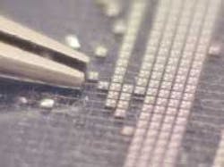
Between these processes are device-preparation steps that include cleaving wafers into bars, optical inspection, facet coating, singulation into die, characterization testing, and sorting. Currently, these processes are much less advanced than the wafer-fabrication and packaging steps—in a typical laser-diode fab, operators perform many steps manually while handling the tiny devices with tweezers or vacuum wands. This inherent lack of process control can result in poor yields and low throughput (see Fig. 1). Because laser-diode bars and dies are very fragile, handling operations should be reduced or consolidated whenever possible. When device handling is unavoidable, precision automated equipment can produce consistent results and improve yields.
Creating facets
During production of laser diodes, facet coating is done while the devices are still in bar form. Typically 10 mm long, the width of bars is defined by the laser cavity between the facets. The bars are cleaved by diamond scribing of the wafers along a crystal-lattice plane to provide parallel facets. These facets are subsequently coated with reflective and antireflective thin films to create mirrored surfaces with the desired front and backside reflectivity. After coating, bars can be scribed and broken into die. Inspection and testing is performed before dies are ready for final packaging.
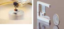
The cleaving process begins with substrates mounted on film frame carriers. Tape selection for these carriers is critical as it must hold the wafer securely during cleaving, but not so tightly that bars are difficult to separate from the tape during pick-and-place (see Fig. 2). The bars are formed by scribing and cleaving the width, turning the frame 90°, and then cleaving the length.Pick-and-place of the bars and small die is not a trivial task. A motorized die-eject mechanism uses needles to push the targeted bar or die up, while holding the surrounding tape down with a vacuum. This allows the tape to peel away from the bottom surface. Then the vacuum pick-up tip picks the bar or die off the tape. Several parameters of this process must be optimized to ensure a successful pick without causing damage to the device. Critical parameters are needle lift height and speed, pick-up tip positioning, and pick-up speed. The main objective is the requirement that the tape stretches around the rounded tip of the needle to reduce the surface area in contact with the underside of the bar or die. To avoid any damage, the needles should not pierce the tape.
As noted, tape selection is also critical to success. The degree to which the tape will stretch while retaining its adhesion varies with grades and manufacturers. With some tapes, stretching assists in reducing adhesion to better facilitate picking. In general, the tape should not be stretched excessively—just enough to separate the bars or die such that adjacent facets do not contact each other during the eject process. Experimenting with different film types while having a solid understanding of the mechanics of the pick-and-place process can help a production engineer achieve optimum performance.
Stacking
The bar stacking pick-and-place system must be capable of interleaving bars with spacers that are either wider or narrower than the bars to promote specific coating effects on the facets. The system must also allow extra spacers to be placed at the top and bottom of the stack. The precision of the stacking process enables the system to align the bars and spacers to either one edge or to the center. Spacers tend to be wider than bars to ensure that no coating is deposited on metallized p or n surfaces, which must remain conductive.
Coating fixtures are used to hold a stack of, for example, 10-mm-long bars with facet surfaces exposed in an evaporative coater. Standard fixtures can hold stacks of bars up to 14 mm high and are available to hold bars with device lengths from 250 to 3000 µm. Custom fixtures are available for other sizes.
Many coating chambers will accept eight or more stacked fixtures to be processed at one time. The fixture securely holds the stack of bars during handling and can be flipped so that both sides can be coated during one pump-down cycle. Fixtures are designed to prevent shadowing and their stainless-steel construction allows chemical cleaning of built-up deposits. After both facets of the bars are coated, the fixtures are unstacked. The coated bars can be placed back onto a film frame or to Gel Pak. The spacers, having served their intended purpose, are usually discarded.
Die singulation and testing
After bars are cut into individual die, each die must be ejected and picked from the tape and placed into a carrier tray for packaging. Because most of the total cost of a finished laser diode is in the packaging, known good die should be identified before these expensive processing steps take place. To screen out bad devices and sort based on inspection or tested performance, die can be visually inspected for defects under high magnification and subjected to light-intensity current-voltage (L-I-V) testing. During these characterization processes, handling steps that risk damage to the fragile die should be minimized.
Our approach to laser-diode die pick-and-place uses a conductive vacuum pick-up tip, which picks the die and is also the probe for contacting the top surface. The probe tip delivers the die to a similar stationary probe tip on the test stage. Both probes are connected to a source meter via shielded coaxial cables. The die is lowered to the fixed probe tip until its bottom surface makes contact with the stationary probe to complete the circuit. The test stage incorporates a mounted photodetector that can be positioned close enough to the die to capture 100% of the light emitted by the diverging output beam of the laser.
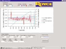
Our L-I-V test system takes advantage of the pulse-mode testing capabilities of third-party source meters (see Fig. 3). This allows laser diodes to be subjected to low-duty-cycle current sweeps to minimize power dissipation and avoid destructive self-heating. Pulse testing is desirable for bar or die testing when external cooling is impractical; it can be accomplished without active temperature control, attachment to submounts, or further investment in die packaging steps. In concert with the source meter, we can perform both DC and pulsed L-I-V sweeps and provide drive current above threshold values to the lasers for spectral analysis. As the source meter provides drive current to excite the laser, it simultaneously measures the output of the laser to the photodetector, as well as the forward voltage at the probe tips.The data collected must be available for display and analysis, and the control limits for performance parameters should be adjustable via a user interface. Finally, tested devices can be sorted into output bins.
Inspection
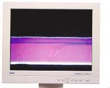
A good laser-diode testing system must also include the ability for an operator to visually inspect the p side of bars and die. It may also be necessary to inspect the facet surfaces of devices for mechanical or coating defects and contamination (see Fig. 4). This should be done with high-magnification optics, a color CCD camera, and monitor. Facet-inspection modules include the ability to rotate bars and dies 180°, make fine angular corrections to align the facet plane perpendicular to the optical axis, and the ability to automatically position the inspection stage to continuously scan the length of a bar or index to the emitters. Nomarski (or differential interference contrast) optics are widely used for inspecting facets because they allow for easier identification of spatial flaws that may not be visible with conventional optics. Nomarski optics are most commonly used to inspect for dislocations in the crystal-lattice plane.Future growth in applications of compound-semiconductor edge-emitting laser diodes for communications and other markets will be significantly influenced by manufacturing costs. Laser-bar producers can benefit by automating steps that are difficult to do manually and eliminating some handling steps, thus improving efficiency, throughput, and yields. Testing and inspection at the die or bar level can effectively screen defective die so that only known good die advance to the cost-intensive final packaging step.
Lisa Gerbracht is head of applications engineering at Royce Instruments, 500 Gateway Dr., Napa, CA 94558; e-mail: [email protected].


