InGaAs sees infrared and visible light
TARA MARTIN and PETER DIXON
Newly developed indium gallium arsenide arrays sense light over a wavelength range of 400 to 1700 nm, making them a prime choice for applications such as night vision, inspection, and agricultural sorting.
The ability of indium gallium arsenide (InGaAs) photodiodes to operate at room temperature with high quantum efficiency for wavelengths from 920 to 1700 nm makes InGaAs an optimal material choice for short-wavelength-IR (SWIR) imaging applications. These applications span commercial and industrial opportunities such as semiconductor-wafer inspection, wavefront sensing, astronomy, spectroscopy, and machine vision. In the military, applications range from covert surveillance to active pointing and tracking and laser radar. Recently, In0.53Ga0.47As photodiode arrays (PDAs) capable of simultaneously detecting visible (400-750 nm), near-IR (750-1000 nm), and SWIR (1000-1700 nm) wavelengths have been developed. This technology enables a single array to do a job previously requiring two arrays and complex system integration including beamsplitters and specialized optics. The dual-wavelength-band InGaAs arrays achieve the same low dark current as commercial SWIR InGaAs arrays.
Frontside or backside illumination
Traditional SWIR InGaAs PDAs, as well as the newly developed visible-SWIR InGaAs PDAs, are hybridized to CMOS readout integrated circuits (ROICs). The resulting focal-plane arrays (FPAs) are then integrated into cameras for video-rate output to a monitor or for use with a frame grabber in a computer for quantitative measurements and machine vision. Popular InGaAs FPA geometries include 320 × 240-, 320 × 256-, and 640 × 512-element arrays with pixel pitches from 25 to 40 µm.
The traditional epitaxial structure for InGaAs p-i-n photodiodes consists of an n-type indium phosphide (InP) substrate, followed by an intrinsic InGaAs absorption region, and topped off with an InP cap. The photodiodes can be either front- or backside illuminated. Single-element photodiodes and 1-D arrays are most often frontside illuminated, while 2-D arrays are backside illuminated because of the indium-bump-bonding process used to integrate the arrays with a CMOS readout circuit. In the case of backside-illuminated arrays, a “planar/mesa” process is used in which the individual photodiodes are planar with all the processing done through holes in a passivating silicon nitride coating. The entire photodiode array is isolated on a mesa that allows frontside electrical contact to the common-cathode substrate.
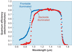
In a frontside-illuminated format, light must pass through the InP cap to reach the InGaAs absorption region, while in a backside-illuminated format, light must pass thought the InP substrate to reach the absorption region. Typically, the InP cap is on the order of 1 µm thick while the InP substrate is on the order of hundreds of microns thick. The quantum efficiency of frontside- and backside-illuminated photodiodes is the same for wavelengths greater than 1100 nm for both diodes, but the quantum efficiency of the frontside-illuminated diode is greater for wavelengths below 1100 nm (see Fig. 1). This higher quantum efficiency is due to the thinner InP layer that the light passes through before reaching the active InGaAs region in the frontside-illuminated format. In fact, the ability to vary the thickness of the InP window layer previously enabled InGaAs linear arrays to be used within the visible spectrum.1
The bandgap of InP is 1.35 eV, corresponding to a cutoff wavelength of 920‑nm. The bandgap of lattice-matched InGaAs is 0.75 eV, corresponding to a cutoff wavelength of approximately 1700 nm. While the InGaAs on its own responds to both visible and SWIR wavelengths below 1700 nm, the InP cap (for frontside-illuminated devices) or substrate (for backside-illuminated devices) absorbs the wavelengths below 920 nm, resulting in only wavelengths greater than 920 nm reaching the InGaAs active region. It is the InP absorption below 920 nm, not the capabilities of InGaAs itself, which until recently has limited InGaAs FPAs for visible imaging.
Thinning the substrate
Thinning or removing the InP substrate achieves increased quantum efficiency in the visible wavelength band in the InGaAs layer.2 For a backside-illuminated FPA, just enough InP to passivate the InGaAs surface and provide a contact layer for the frontside common-cathode contact is needed. This results in an FPA consisting of just the epitaxial layers bump bonded to a CMOS ROIC. The quantum efficiency for an InGaAs array with the very thin InP layer at 700 nm is now 50% (see Fig. 2). This is almost a factor-of-five improvement over even that for the frontside-illuminated detector. At 500‑nm, quantum efficiency is approximately 20% versus less than 1% typically seen for standard frontside- or backside-illuminated photodiodes at 500 nm. This thinner layer achieved with etching and mechanical thinning is thinner than that achieved by mechanical thinning only. Thicker InP layers lead to lower quantum efficiencies in the visible spectrum, as well as to image retention.3 The image retention most likely arises from photoluminescence from the InP, which absorbs visible light and readmits it as photoluminescence; this process is slow, with a time scale on the order of video-rate imaging.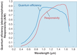
Having a single FPA that can image both in the visible and SWIR wavelength bands is of interest for applications that currently require two separate cameras to image the two wavelength bands. Having a single camera simplifies image-fusion systems and decreases payload size and weight. Focal-plane arrays made with InGaAs are widely used for night-vision applications because of the SWIR light available at night. Indium gallium arsenide performs far better than image-intensified CCDs at night, but standard InGaAs arrays are not able to see some standard laser designators used by the military. The new visible-SWIR InGaAs arrays can see all commonly used laser designators (800- to 900-nm lasers, as well as 1310-nm communications lasers and eye-safe 1550-nm lasers). Combined visible-SWIR capabilities are also of interest for hyperspectral-imaging applications. The visible response should also assist InGaAs nighttime capability by detecting more of the available photons-that is, visible and SWIR instead of one or the other.
Short-wavelength-IR cameras provide high-contrast daytime images, but because they cannot see visible light, they cannot image details that are painted or printed for use in the visible, such as signs, paintings, fabric patterns, and vehicle lettering. In addition, SWIR cameras cannot view television or computer monitors because the imagery consists of only visible light. In some applications, and in particular for military-surveillance applications, having the ability to see details on signs, fabrics, and computer monitors, as well as to see all laser-designator wavelengths or perform nighttime imaging is important (see Fig. 3).
Uses in industry
In commercial applications, visible-SWIR cameras can assist in machine vision as well as in hyperspectral imaging. The same array can allow multiple “colors” across two wavelength bands to be imaged by one camera. This simplifies the optical system necessary as well as the processing power required to analyze and compare two camera images. Areas of interest are in agricultural sorting, for which defects are not necessarily apparent in the visible spectrum; and inspection applications, in which visible attributes need to be simultaneously observed with hidden nonvisible attributes. One example of the latter is pharmaceutical bottles, where labels need to be read by users but tamper-resistant protections meant to stay hidden are written in ink that is detectable in the near-IR and SWIR bands only.
Further improvements to visible-SWIR InGaAs arrays are expected over the next one to two years. One such improvement will include optimizing the epitaxial wafer structure to increase quantum efficiency throughout the visible-wavelength band.
REFERENCES
1. J. B. Williamson et al., IEEE Transactions on Electron Devices 38(12) 2707 (1991).
2. M. H. Ettenburg et al., LEOS 1999. IEEE Lasers and Electro-Optics Society 1999 12th Annual Meeting (1999).
3. T. R. Hoelter and B. B. Barton, Proc. SPIE 5074, 481 (2003).
Tara Martin is a research engineer and Peter Dixon is a senior processing engineer at Sensors Unlimited Inc., 3490 U.S. Route 1, Bldg. 12, Princeton, NJ 08540; e-mail: [email protected].