Charge-coupled devices capture image information
How CCDs work
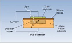
A CCD array is built up out of pixels, each consisting of a metal-oxide-silicon (MOS) capacitor. Each of these is an insulating silicon dioxide layer over a p-type silicon substrate, capped by a thin metal electrode (see Fig. 1). When bias is applied, holes move away from a depletion layer in the silicon beneath the gate, creating a potential energy well. Electrons generated when the device is illuminated accumulate in this well; the charge accumulated is proportional to the irradiation.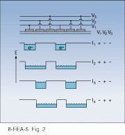
This is the simplest readout system—line address; it has the disadvantage that capacitors are accumulating more charges through exposure to light during transfer cycle, leading to a smearing of the image. For low light levels, where exposure times are very long relative to readout times, this is no problem, but for quick exposure times, a shutter has to be used during charge transfer.
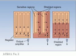
To avoid this problem, other transfer approaches are used. In interline transfer, each column’s capacitors shift its charge during readout to an adjacent column that is shielded from light. Transfer off the array then occurs through the shielded columns while the next exposure is made. Of course, this arrangement eliminates about one-half the space available for ex posed pixels. A third alternative is frame transfer, in which a quick transfer occurs from the active pixels to a shifted array, which then reads out at a slower pace, as required by multiplexed electronics.
In certain applications, the problem of image smearing can be eliminated by actually moving the image across the array in synchronization with the readout, so that as the charge shifts from pixel to pixel, the same part of the image is always being exposed. Such time-delay-integration schemes allow readout of data at a steady pace, rather than in bursts, as well as maximizing exposure times as a fraction of total time. Modifying the clocking scheme, from three-phase to two- or four- phase, adds to CCD versatility and allows for electronic shuttering, iris control, and image scanning.
Arrays can either be oriented so that illumination comes through the electrodes, termed frontside illumination, or so it falls directly on the semiconductor, termed backside illumination. For frontside illumination, the electrodes themselves must be made transparent, which is done by making them from extremely thin silicon, heavily doped for electrical conductance. However, transparency drops for violet and ultraviolet (UV) photons shorter than 0.41 µm. When this is important to the application, electrodes also can be made from more transparent materials such as doped indium tin oxide.
Backside illumination eliminates these problems but generates a few of its own. In the blue and near-UV spectral region, the problem is that the absorption lengths are so short—typically around 0.3 µm for wavelengths of 0.4 µm—that photoelectrons are formed only very near the surface of the capacitor. However, if the capacitor is thinned to around 15 to 20 µm, sufficient electrons will diffuse into the depletion region for good efficiency. Because at wavelengths of 1 µm the absorption length is up to 80 µm, such thinned CCDs lose sensitivity in the near-IR. Nonetheless, CCDs can be tailored to operate anywhere from x-ray wavelengths up to a limiting wavelength around 1.1. µm—the cutoff for photoelectron production in silicon.
There are a number of techniques for improving CCD performance at short wavelengths. One is to flood the CCD with intense UV light before exposure. The UV photons cause the emission of electrons in the bulk silicon, and some of these migrate to the backside surface, where they are trapped in the oxide layer there. These create a negative potential that pushes photoelectrons emitted during exposure toward the storage wells. Gases such as chlorine or nitric oxide produce similar results.
The biggest reason for the popularity of CCDs is their high sensitivity. In many situations, CCDs approach 100% photon-to-electron efficiency. The only source of noise in CCDs is the thermal generation of electrons, which limits total signal to noise levels and thus sensitivity. Even at room temperature, however, noise levels are often negligible relative to avoidable light, and, for low light applications, thermal noise can be reduced by cooling the CCD itself. At liquid-nitrogen temperatures, for example, used in applications such as astronomy, dark currents can drop as low as one electron per pixel per hour, and even at -45°C, dark currents are only around ten times this level.
The operation of a CCD also allows sensitivity to be traded for resolution by binning several pixels together during readout. Although CCDs themselves can view near-IR radiation to about 1.1 µm, their range can be extended by combining them with other technologies. For example, night-vision cameras used at room temperature link CCDs with gallium arsenide image-intensifier tubes (see Laser Focus World, May 1996, p. 32). Here, a GaAs photocathode generates photoelectrons from short-wavelength IR radiation. Electrons are multiplied by a multichannel plate, with the electrons producing secondary showers from the walls of each channel. The electrons then are converted to visible light as they strike a phosphor, and a CCD mounted behind the phosphor records the visible light image. Such combinations, however, are limited in resolution because spot size tends to be at least 100 µm and efficiency is relatively low.
Given the ubiquity of CCD technology, manufacturing benefits from large-scale production, so CCD processing tends to be on the cutting edge of semiconductor fabrication techniques. Wafer-scale CCDs are now relatively mature, with the largest arrays produced having 25 million or more pixels.
Faster and smarter
While CCD technology is relatively mature, there are a number of areas in which significant improvements are being made. One bottleneck to CCD-array operation, as with any array sensor, is the readout rate. Reading out the pixel exposures involves analog-to-digital conversions, and the faster the readout rate the higher the read-noise level that is introduced. Thus, for a given signal-to-noise level, the readout rate is limited, which can constrain frame rates, a major problem for extending CCDs into applications that require recording fast responses. For example, with a 2-MHz readout rate, a typical 512 × 512 array can only be run at eight frames per second. In practice, this rate cannot be achieved, because time has to be allowed for charge transfer and exposure.
Two techniques overcome these limitations. First, binning, often used to increase signal-to-noise ratio, can improve frame rates, trading space for time resolution. Second, the frame-transfer design can decouple charge transfer out of the exposed array of pixels and the readout from the storage array. Together, these techniques can give users a good deal of flexibility in choosing the right balance among time resolution, frame size, spatial resolution, and signal-to-noise ratio or sensitivity.
For some applications, such as biological studies of calcium-ion concentrations in nerve cells, frame rates as high as 100 frames per second may be needed. Frame-transfer CCD arrays can be programmed to digitally cut the 512 × 512 exposed array into ten slices, each being exposed separately for a short time. Then the whole exposed array is transferred in 1 to 2 ms to the storage array. While another 10 miniframes are acquired, the signal storage array is read out.
Another area of advance is in dynamic range. At room temperature, CCDs have dynamic ranges of a few thousand—basically similar to maximum signal-to-noise ratios. But typical scenes may have dynamic ranges of 100,000 to a million. For the human eye, such dynamic ranges are not a challenge, because the eye adjusts its sensitivity from point to point on the image, allowing human dynamic ranges of as high as 100 million. Lack of dynamic range in photographic media has always been a problem and leads to the great difference in the way, for example, a camera records a scene and the way the human eye sees it. Large amounts of information are lost in a photographic recording or a CCD picture because luminances are too little or too great in parts of the scene.
The flexibility of CCD technology may lead to some solutions for this problem. Recent work by Sarit Chen and colleagues at the Technion – Israel Institute of Technology (Haifa, Israel) is aimed at developing CCDs in which each pixel automatically regulates its sensitivity to the amount of light falling on it by adjusting its exposure time. A reset gate controls the exposure time, cutting it to prevent pixel saturation. This configuration also avoids blooming, where charge spills from a saturated pixel to neighboring ones. (Exposure rates are set on the basis of the luminosity at the pixel during the preceding frame.)
At the the end of the frame exposure, readout occurs conventionally, but the exposure times for each pixel are read out into the processing equipment as well. Various algorithms to compress the dynamic range to fit with that of the output or recording medium can then be used. This contrast-reduction scheme both produces scenes similar to that the eye would see and preserves information that would otherwise be lost in black or white regions of the image.
About the Author
Eric J. Lerner
Contributing Editor, Laser Focus World
Eric J. Lerner is a contributing editor for Laser Focus World.