Choosing a detector for your light-sensing application
LARRY GODFREY
Many factors are involved in choosing a detector for a given light-sensing application. The choices may seem overwhelming and include photodiodes, phototransistors, photodarlingtons, photomultiplier tubes (PMTs), photoresistors, and integrated circuits, in addition to various hybrids and even thermopiles. The optimal approach involves consideration of application-specific parameters such as source wavelength, image size, optical power, signal-to-noise ratio, and package constraints.
Light-sensing options
Applications vary widely, ranging from specialized instrumentation that detects individual photons to measurement of the power output of high-speed welding or cutting lasers that produce kilowatts of optical power. Fortunately, there are sensors for almost any application imaginable—from a PMT that produces a large voltage pulse for each photon it detects to cooled thermopiles that absorb kilowatts of power and produce a thermocouple voltage proportional to the optical power absorbed.
Photomultiplier tubes. PMTs are specialized vacuum tubes that incorporate a light-sensitive photocathode that absorbs incoming photons and subsequently emits electrons. The tube multiplies the number of electrons produced by accelerating them into plates—dynodes—that emit a large number of secondary electrons for each electron that hits them. A cascade arrangement of about ten dynodes provides electron multiplications of up to one million. For a single incident photon, PMTs can produce hundreds of millivolts across a 50-W load resistor at the PMT output.
Photomultiplier tubes offer the ultimate light-detection sensitivity; they can sense individual photons. And, when cooled, a PMT is essentially noise free with, at most, one false photon pulse per second.
There are, however, trade-offs for such high sensitivity. Relative to other detectors, the cost of PMTs is high. They are mechanically fragile, they are limited in their packaging, and they are susceptible to magnetic fields. Their spectral sensitivity is also limited; typically PMTs operate from about 190 to 900 nm, although custom devices are available up to 1100 nm. Furthermore, PMTs require a stable high-voltage power supply.
Photodiodes. The primary differences between photodiodes and standard semiconductor diodes used in electronic circuits are that the photodiode chips are larger and they are packaged to allow light onto the sensitive area of the diode. The advantages of photodiodes—in terms of cost and performance—make them almost ubiquitous in today’s “high-tech” society. They are found in personal blood-sugar monitors as well as in load levelers in luxury cars. Assembly-line sensors, domestic smoke detectors, and cranial pressure sensors for head-injured patients are just a few of the many other applications.
Silicon-based devices cover a wide spectral range from 190 to 1100 nm (the lower limit is set by absorption of UV light in air). Germanium-based photodiodes overlap the spectral response of silicon-based devices and are usable to about 1600 nm. Other semiconductor materials, including compounds of gallium, arsenic, indium, antimony, and phosphorous, can be fabricated into photodiodes to cover small sections of the 190- to 2000-nm spectral range. The fiberoptics industry, for example, uses an indium gallium arsenide detector for sensing in the 1000- to 1500-nm range. More exotic photodiodes extend spectral coverage beyond 2000 nm up to 3000 nm.
Photodiodes are available in standard packages, or they can be custom-made to a specific design at relatively little extra cost. They are small, lightweight, and relatively inexpensive, with million-piece pricing as low as $0.25 each. These devices can measure optical power from only a few picowatts up to milliwatts with reproducible sensitivity and risetimes as fast as 10 ps.
Photodiodes do need an operational amplifier or similar circuit to give signal gain for picowatt-level applications. At high optical-power levels (greater than 10 µW), a simple load-resistor configuration can give adequate performance and also can provide TTL (transistor-transistor logic) voltage compatibility. If noise is a problem at low light levels, an avalanche photodiode will provide internal current gain of up to about 100.
Phototransistors and photodarlingtons. Though similar to their electronic-signal-device counterparts, phototransistors are designed to measure light, so they are assembled in a transparent package. Phototransistors may be more convenient than photodiodes because of their built-in gain; absorbed light creates a current in the base of the phototransistor that results in current gain from 100 to several thousand. Photodarlingtons, with two gain stages, provide net gain that can exceed 100,000.
The built-in gain allows a phototransistor to be coupled with a load resistor, thereby providing TTL compatibility over a wide range of light levels. Coupled with ease of use and low cost, this compatibility has made phototransistors popular for applications involving more than a few hundred nanowatts of optical power.
These devices, however, do have drawbacks compared to photodiodes. The frequency bandwidth and linearity are relatively limited, and spectral response is restricted to between 350 and 1100 nm. In addition, there are large variations in sensitivity between individual devices and few standard package options.
Photoconductive sensors. Photoconductive sensors are thick-film semiconductor materials that decrease electrical resistance with increasing incident light. They are typically less than 0.25-in.-diameter rugged assemblies that can withstand hundreds of volts. Photoconductive sensors based on cadmium sulfide (CdS) have spectral sensitivity curves that approximately match the sensitivity of the human eye, so they are useful for applications that involve mimicking human perception of light, such as headlight dimmers or intensity adjustments on information displays.
These sensors can be designed for measuring microwatts to milliwatts of optical power and are very inexpensive at high volume (less than $0.10 each). Such characteristics make CdS-based photoconductors the sensor of choice in applications such as street light control and in the toy industry.
There are, however, considerations that limit use of CdS-based photoconductive sensors in more sophisticated applications such as those requiring sensitivity over a wide spectral range, small variations between individual parts, or no history-dependent response. The resistance of these sensors depends on the thick-film microstructure, so the resistance specification has a wide tolerance—typically a range from maximum to minimum of three or more. The resistance also has "long-term memory"; it depends, at any given time, on the amount of light actually incident on the sensor plus the sensor`s light history for the past several days.
Photoconductors made from materials other than CdS, such as lead telluride and mercury cadmium telluride, are also available. These materials have spectral sensitivities that cover the range photodiodes do not: above 2000 nm and out to 15,000 nm. This longer-wavelength sensitivity is important for IR imaging cameras and for long-wavelength instrumentation such as is used to monitor carbon dioxide laser emission and atmospheric physics. These sensors tend to be more expensive than both silicon photodiodes and CdS photoconductors.
Integrated circuits. Incorporating additional electronics directly onto a semiconductor sensor chip makes it possible to add additional functions to the sensor. An “optical IC” is an integrated circuit comprising photodiode and electronic-signal-processing circuits. Such additional functions as current-to-voltage conversion and reference-level sensing (a Schmitt trigger, for example) can be incorporated. Other optical ICs can provide signals highly immune to noise, such as a current-to-frequency conversion.
The principal advantages of an optical IC are ease of use, small size, and immunity to electronic noise compared to a photodiode with separate electronics. Typically these devices are much more expensive and offer a very limited active light-sensing area. Custom tooling for specific applications is also expensive.
Hybrids. The electronic functions of an optical IC can also be provided by a hybrid circuit that has unpackaged IC components attached directly to a substrate that also holds a photodiode. This type of sensor combines the ease of use and immunity to electrical noise of an optical IC with increased design flexibility and lower tooling costs. In addition, the sensitivity can be easily increased with a larger photodiode area without paying for an IC of the same area.
The primary disadvantages of a hybrid sensor are its cost and reliability. Cost can be several times higher than the electronic-assembly option discussed below, and reliability is an issue at low production volumes. In this case, the high cost of lot-related reliability testing is difficult to amortize, so either limited reliability screening is implemented or the piece cost becomes high.
Sensor electronic assemblies. Combining any of the sensors listed above with printed-circuit-board-based electronic signal processing creates sensor assemblies or "black boxes." The user defines specifications for light input and the desired output response; the vendor builds and tests the system to ensure that the specifications are met. An assembly can also include optical components such as lenses and wavelength filters. The user just bolts the assembly in place and connects it to the high-level electronics; there are no concerns about mismatch between the purchased sensor and front-end amplifiers or diagnostic electronics. The system is relatively immune from noise and is highly reliable because of the mature manufacturing technologies used.
Sensor electronic assemblies are easy to use. Experienced vendors can often deliver better reliability and lower cost compared to a designer’s in-house manufacturing. Less flexibility in making changes “on the fly” is the main disadvantage, but this is not an issue for a responsive vendor or mature designs.
Other sensors. There are many other types of sensors. These include avalanche photodiodes, bolometers, self-scanned arrays, and photon drag detectors. A sensor vendor can provide information about these devices and can discuss the physics of each detection technology.
Selecting a sensor
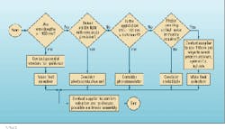
Reviewing a few key design aspects generally provides enough information for making an optimum choice of detector for a given application (see figure).
For sensing of wavelengths below 1100 nm, photoconductive cells or a silicon-based detector should be appropriate. At wavelengths above 1100 nm, the costs and technology options are not straightforward, and a detector vendor consulted at the beginning of a design program will provide effective guidance.
Photoconductive cell. Applications at visible wavelengths with at least microwatts of optical power, in which the sensor is simply required to detect if light is present, can use one of the least expensive and most rugged detectors available--the photoconductive cell. There are many standard devices and custom-design options including electronic assemblies.
Silicon phototransistor. Silicon phototransistors, the second-lowest-cost sensors, are also convenient and should be considered next. At least nanowatts of optical power within a 1-mm-diameter spot are required at wavelengths between 350 and 1100 nm. The application must also tolerate unit-to-unit sensitivity variation.
Silicon photodiode. For UV to near-IR wavelengths, photodiodes offer the best overall performance. They are only slightly more expensive than phototransistors, but their spectral range is broader, and they have lower noise, more uniform sensitivity and reproducibility, a larger dynamic range, better linearity, and more package options. Thus, if phototransistors or photoconductive cells are not appropriate for an application, more often than not a photodiode will suffice.
Other options. At least 90% of detector applications should be satisfied by one of the sensors discussed above. However, when light levels are extremely low, ambient electronic noise levels are very high, or space requirements are particularly limited, other alternatives, such as optical ICs or hybrids, should be investigated.
After selection, develop a partnership with your sensor vendor. The vendor is the sensor expert, and working together can help create a successful project design. Most important, supply the vendor with specific application information about technical specifications, ambient light levels, operating lifetime, operation and storage environment, project schedules, anticipated production volumes, and cost targets for tooling and unit price. With this information the sensor vendor can help a system designer make informed recommendations after considering trade-offs between reliability, technical performance, and cost.