Applications drive new detector technologies
Although detector technology is a relatively mature field, it continues to undergo rapid change. New types of devices based on superconductivity may soon allow scientists to detect a source’s spectrum and image it at the same time, without filters or gratings. New materials are reducing cooling requirements, leading toward room-temperature, background-limited infrared (IR) detectors. And, the widespread charge-coupled-device (CCD) sensor may face stiff competition from active-pixel sensors, leading to cheaper and smaller video cameras.
Superconducting detectors
The discovery of high-temperature superconducting (HTS) materials in 1986 led to a rush to find applications, and optical and IR detectors were among the first ones studied. Because these superconductors operated at liquid-nitrogen temperatures, as did many types of IR detectors, the choice was natural. As with other HTS applications, achieving practical results was not easy, and commercial success has not yet been achieved, but new developments, such as the HTS bolometer developed at Conductus (Sunnyvale, CA), may change that (see Laser Focus World, Nov. 1996, p. 11).
Two characteristics make HTS technology attractive: the very low energy gap in such materials makes them ideal for IR detection, and superconductors have extremely low energy generation, so they can operate at high speeds without being warmed up. As with semiconductors, superconducting detectors can operate as bolometers—relying on small changes in temperature—or as quantum detectors—relying on individual photon interactions. As the resistivity of superconducting material rises very rapidly from zero, near the transition temperature, they can be very sensitive to minute changes in temperature (see Fig. 1).1 Such superconducting bolometers can compete with semiconductor bolometers at wavelengths longer than 20 µm and have the advantage that they need only liquid-nitrogen cooling, while semiconductors for the same wavelengths generally require liquid-helium temperatures.
Among superconducting quantum detectors, perhaps the best know is the Josephson junction. In this device, for even longer wavelengths into the submillimeter and millimeter range, nonlinear interactions between an incoming photon and the high-frequency oscillation in the junction produce a signal. Other approaches use superconducting quantum interference devices or measure changes in other electrical properties of a superconductor. All these approaches, however, have faced serious technical challenges and generally have not shown improved performance over semiconductors.
This situation may be changing with the announcement in May 1996 of good results with a new type of superconducting device—the superconducting tunnel junction (STJ)—that works with conventional, rather than high-temperature, superconductors. The great advantage of STJs is that they can detect not just the number of photons absorbed, but the energy of each individual photon as well. In astronomy, in particular, but in many other applications as well, it has been a long-term goal to gather spectral information, imaging, and timing information at the same time, but, there are difficulties in doing this simultaneously with CCD technology.
Timing information can only be achieved by short exposures, which cuts sensitivity, while spectral information requires either gratings to spread out the light for a given point source or filters to gain some spectral information over an entire image. In STJs, however, the time of arrival of individual photons can be detected, and the number of electrons released by each is proportional to the photon energy, so an array of STJs can give all four dimensions of information at once. There is one large catch: STJs need to operate at very low temperatures, below 1 K, so the devices must use conventional superconductors.
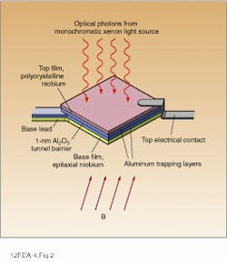
An STJ consists of a sandwich of aluminum oxide between two layers of niobium, with additional layers of aluminum between each niobium layer and the central aluminum oxide. When a photon of radiation is absorbed by the top niobium layer, the photon breaks up the Cooper pairs of electrons that maintain superconduction, producing free electrons. The higher the energy of the photon, the more free electrons are produced. These free electrons then tunnel across the aluminum oxide barrier, driven by a bias voltage. A small magnetic field prevents the superconducting Cooper pairs from also tunneling. So the electrons, which are trapped in the alumina layers, create a current proportional to the energy of each photon (see Fig. 2).Initial experiments, performed by a team of researchers in Great Britain and the Netherlands working at the European Space Agency and Cambridge Microfab Ltd. and Oxford Instruments (both in Cambridge, England), yielded modest spectral resolution of 45 nm at wavelength of 350 nm.2 But improvements can better that resolution at least fivefold, and the STJ boasts quantum efficiencies of 50% over the band from 200 nm to 1 µm. Arrays of such STJs could be used in the future on space instruments such as the Hubble Space Telescope to produce spectra of thousands of the faint galaxies. Such spectral data will yield both the galaxies` distances and the age of their stars, vital data in understanding the evolution of the cosmos. Francesco Parece of the European Southern Observatory says, "This promises a true revolution in the way astronomers work."
Room-temperature IR detectors
Superconductors, whether high-temperature or not, require cooling, as do most IR detectors. However, new materials and approaches are now making possible IR detectors that give background-limited performance at room temperature. The key to this development is the reduction of thermal generation and recombination of electron-hole pairs. There are a number of ways to do this. The simplest is to reduce the thickness of the detector, thus reducing the potential number of electrons available for thermal generation. Because thinner detectors have less absorbency, quantum efficiency must be maintained by techniques such as backside reflectors, which double the path length through the detector.
A second approach is to concentrate the light by putting the detector inside a hemispherical lens. This improves signal-to-noise ratios, because again thermal generation is proportional to detector bulk, while the signal strength increases with optical concentration.
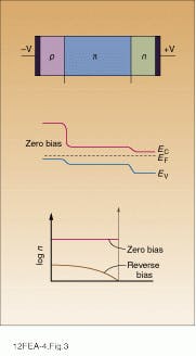
In the past year or so, some more-sophisticated approaches, combined with the earlier techniques, have approached room-temperature, background-limited performance in at least parts of the IR spectrum. One of these new approaches is based on a nonequilibrium mode of operation. The idea in this approach is to decrease the concentration of free carriers below its equilibrium value. This condition can occur with light doping, under conditions of strong depletion. In a typical design, the photodiode consists of three layers: the first is a wide-gap n-type, the second a narrow-gap, lightly doped p-type, and the third a wide-gap p-type (see Fig. 3). When the diode is reverse-biased, the junction between the p and n layers extracts electrons, which cannot be replaced, so the electron density throughout the central layer drops by more than a thousandfold. This drop, in turn, greatly suppresses thermal generation of current, because noise generation goes as the square of the carrier density.Photovoltaic detectors using this technique, based on research in Great Britain and Poland, are now being manufactured in Poland and sold in the USA by Boston Electronics Corp. and Oriel (Stratford, CT). These devices are made with a quaternary compound, mercury cadmium zinc telluride (MgCdZnTe), in which zinc is added to the standard IR-detector material mercury cadmium telluride (HgCdTe). The addition of zinc actually eases manufacture by improving the match of the final material to the underlying binary substrate and reduces defects that add to thermal noise. The detectors use light concentration to increase signal-to-noise ratios, and they also benefit from the "Dember effect," in which charge separation of electrons and holes is achieved by the far greater mobility and lifetimes of the electrons.
While the detectors have not yet achieved background-limited performance at room temperature, with only thermoelectric cooling they can exceed the sensitivity of HgCdTe detectors cooled by liquid nitrogen for high-frequency signals and match the performance of liquid-nitrogen-cooled indium antinomide (InSb) at all frequencies. Jozef Piotrowski, director of Vigo Systems Ltd. (Warsaw, Poland) and one of the key researchers in the field, says that he expects to achieve background-limited performance of HgCdZnTe at room temperature within a few years.
Active-pixel sensors bounce back
Perhaps the development with the broadest significance is the introduction of imaging detectors using active-pixel sensors (APSs) as a replacement to ubiquitous CCDs. At present, CCDs are the workhorse of all electronic imagers from the humble camcorder to the Hubble Space Telescope. But CCDs have certain drawbacks. Because they transfer charge many times to get to the edge of the array, they require an extremely high level of perfection in fabrication. This characteristic makes them vulnerable to relatively low levels of radiation, a disadvantage for space applications. They also require relatively power-hunger auxiliary circuits for timing and the voltage shifts needed to transfer the charges, and these auxiliary circuits prevent high degrees of miniaturization.
In addition, CCDs cannot be produced on conventional CMOS microelectronics production lines—they need their own special-purpose semiconductor-production process. This increases costs through reduced volume and limits manufacturers to a few, almost exclusively in Japan, that produce CCDs for their own products.
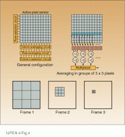
Potentially, active-pixel sensors can overcome these drawbacks. In active-pixel sensors, individual photodetectors, similar to the single pixels in a CCD, are integrated with individual transistors (see Fig. 4). This configuration means that the array can be read out over wires like random-access memory, rather than by shifting charge repeatedly from one pixel to the next, as in a CCD. Such APS devices can be produced on conventional CMOS production lines, taking advantage of the huge production volume of electronic chips. Active-pixel sensors can integrate all functions—detection, amplification, and timing—onto a single chip, allowing for great miniaturization, and they can reduce power requirements by orders of magnitude. In addition, they are relatively radiation hard, because a defect will only affect a single pixel, not a whole line of pixels as in CCDs.Although active-pixel sensors were first proposed in 1968, they had to await advances in microlithography to become practical. Until linewidths dropped sufficiently that the transistors would not take up more space than the photodetectors, APSs could not compete with CCDs. However, with submicron-scale lithography now standard, that situation has changed. Teams of researchers in the USA and Japan are racing to develop practical APS-based products to challenge CCDs.
At the Jet Propulsion Laboratory’s Center for Space Microelectronics Technology (JPL; Pasadena, CA), a team led by Eric Fossum has developed a 256 × 256 APS with less than 1% the power consumption of a comparable CCD system. While a CCD consumes some 10-20 W of power, primarily in the clock-drive system, the JPL APS, including all functions on a single chip, consumes only about 5 mW. In each pixel of the APS, photons pass through a photogate, generating electrons that are collected and stored beneath the gate. A transistor array reads out the charge amount by the same techniques used in a random-access memory—any individual pixel can be read out in any order.
Currently JPL is developing a 1000 × 1000 APS chip as the heart of a "camera on a chip" small enough to fit into a cube the size of a gaming die. This project, the Digital Imaging Camera Experiment, or DICE, will demonstrate the feasibility of extremely low-cost miniaturized cameras for toys, home security monitors, and video conferencing. A small firm, Photobit (also in Pasadena) headed by Sandra Kemmeny, has been set up to work with product developers. One of the first large markets targeted is video cameras used for video conferencing and attached to PCs. The new technology could bring the cost of such a camera down from around $150 to $20.
In addition, APS-based cameras could be important for space-based applications. For one thing, power reduction could be of use for small satellites, especially planetary probes. In addition, the capabilities of APS to individually adjust the functioning of each pixel can be applied to "smart-sensor" functions such as adaptive exposure times, to allow greater dynamic range, and programmable resolution, to allow sensors to focus in on areas of interest.
Within a decade, active-pixel technology may replace CCDs in many markets, leading to the greatest shift in detector technology since CCDs were introduced.
REFERENCES
1. S. J. Berkowitz et al., Appl. Phys. Lett. 69(14), 2125 (30 Sept. 1996).
2. A. Peacock et al., Nature 381, 1359 (May 1996).
About the Author
Eric J. Lerner
Contributing Editor, Laser Focus World
Eric J. Lerner is a contributing editor for Laser Focus World.


