Understanding the ABCs of detector selection
Understanding the ABCs of detector selection
Earl Hergert
Application requirements, especially light power, frequency bandwidth, wavelength, and cost, will strongly influence choice of detector.
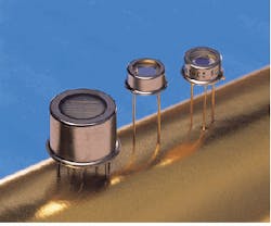
When considering a detector-amplifier combination, it is critical to define the specifications of the application it is needed for, including light power, frequency bandwidth, wavelength, power consumption, and cost. That task can be made easier with knowledge of the different kinds of detector technology--photodiode, avalanche photodiode, and photomultiplier tube (see Fig. 1).
Understanding photodiodes
A silicon photodiode is essentially a p-n junction consisting of a positively doped p region and a negatively doped n region. In between is an area of neutral charge known as the depletion region. When light enters the device, in the photovoltaic operating mode, electrons in the crystalline structure become excited. If the energy of the light is greater than the bandgap energy of the material, electrons will move into the conduction band. This creates holes in the valence band where the electrons were originally located. These electron hole pairs are created throughout the device.
Electron hole pairs generated in the depletion region drift to their respective electrodes--n for electrons and p for holes--which produces a positive charge buildup in the p layer and a negative charge buildup in the n layer. The amount of charge is directly proportional to the amount of light falling on the detector. Connect an external circuit to both electrodes and current will flow in the circuit.
The above describes the photovoltaic method of operation. It is also possible to apply a reverse bias voltage to the photodetector. This condition--the photoconductive mode--increases the electrical field strength between the electrodes and the depth of the depletion region. The advantages of such an operation are higher speed, lower capacitance, and better linearity. However, the dark current is dependent on the reverse bias voltage and will grow larger with increasing bias voltage. Generally PIN (those with a p-n junction) photodiodes and APDs operate in this fashion.
Noise in a photodiode can take two forms. First is the shot noise of the dark current, which results from the statistical uncertainty in the arrival rate of photons. Shot noise is present in all signals and is given by
(1)
where Idark = rms noise current, q = electron charge, idark = dark signal current, and B = frequency bandwidth of detector-amplifier combination.
The second noise source for a photodiode is the thermal noise of the shunt resistance. Also known as Johnson noise, it is given by
(2)
where IRsh = rms noise current resulting from Johnson noise, k = Boltzman`s constant, T = absolute temperature of the photodiode, and Rsh = shunt resistance of the photodiode. The shot noise will dominate in photoconductive operation, while the Johnson noise will dominate in photovoltaic mode.
Basics of APDs
The APD is a specialized silicon PIN photodiode designed to operate with high reverse-bias voltages. Large reverse voltages generate high electric fields at the p-n junction. Some of the electron hole pairs passing through or generated in this field gain sufficient energy (greater than the bandgap energy) to create additional electron hole pairs in a process called impact ionization. If these new pairs acquire enough energy, they also create electron hole pairs. This mechanism, known as avalanche multiplication, is the way APDs produce internal gain, which is an important attribute when the detector is combined with an amplifier.
Because an APD always operates in photoconductive mode, its noise takes the same form as the photodiode dark-current shot noise (see Eq. 1), with the addition of two terms:
(3)
where M = detector internal gain and F = detector excess noise factor. The two additions to Eq. 3 are the gain of the APD and the excess noise factor. The gain amplifies the noise as it would the signal and has no net effect on the signal-to-noise ratio, while the excess noise factor represents noise added to the output signal by the multiplication process. It has a strong dependence on wavelength, as well as gain.
As the light level increases, the dark current no longer impacts the signal-to-noise ratio. Instead, the shot noise of the signal itself tends to dominate the ratio:
(4)
where isignal = photon-generated signal before gain. For applications with strong light signals, the shot noise performance of the detector is of far more importance than detector dark noise and amplifier noise.
Amplifier issues
Probably the most overlooked aspect of detector selection is the amplifier, which usually sets the lower noise floor for the detector-amplifier combination. In a transimpedence amplifier, for example, noise can be broken down into three major components--shot noise, Johnson noise, and voltage noise current. Shot noise of the amplifier input bias current, as a general rule, is much lower than the photodiode dark current and seldom presents a problem. Johnson noise of the amplifier feedback resistor can often dominate the detector-amplifier noise because the value of the feedback resistor must be smaller than the shunt resistance of the photodiode.
The input voltage noise of the amplifier is dependent on the terminal capacitance of the detector and is also strongly related to the frequency bandwidth. The total detector-amplifier noise is a combination of these factors.
Picking photomultipliers
When the light level is low or the signal is of short duration, solid-state detectors often do not have a high enough signal-to-noise ratio to perform the required measurement. The photomultiplier tube (PMT) is well suited for just such a challenge. It is possible to economically construct PMTs with very large surface areas, thereby increasing the amount of light collected or reducing the complexity of the optical system. The device also has an almost noise-free gain as high as 106, but with a small noise factor F of 1.4 to 1.6. By comparison, an APD will have an F of 2 to 4. The very large gain of the PMT often means that the noise of an external amplifier can be neglected.
The designer can, therefore, use the PMT in very low light applications by counting current pulses generated by individual photons. This photon-counting technique has unmatched sensitivity, and, because it is inherently digital in nature, it possesses excellent long-term stability. The PMT is often not considered because designers believe that quantum efficiency or the high voltage (1000 V) supply will complicate the design. This is no longer a concern, however; new photocathode technology (gallium arsenide phosphide and gallium arsenide) is now allowing production of PMTs with quantum efficiencies exceeding 30% and approaching 40% in some regions of the spectrum, and PMT modules that operate at less than 15 V dc are now available.
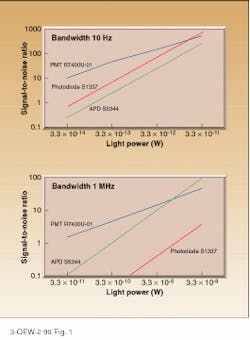
Key to choosing a suitable detector is to list all relevant application requirements.It is also helpful to calculate the signal-to-noise ratio under the conditions of the application. Plots such as signal-to-noise ratio versus light power are convenient for comparing detectors (see Fig. 2). Calculated results can be confirmed by measuring the signal-to-noise ratio in the application itself. While this procedure seems obvious, it is often omitted.
The ultimate test of a detector system is its signal-to-noise performance in a particular application, but this is not the only test to which the detector should be subjected. For instance, in a particular infrared (IR) application, the APD may have the best signal-to-noise ratio, but its large temperature coefficients may make it difficult to use. Here, the designer might prefer the more-stable photodiode despite its lower signal-to-noise ratio. Photodiode, APD, or PMT--the key is to match the detector to application. o
FIGURE 1. Modern manufacturing methods produce detectors of comparable size (from the left, an APD, a photodiode, and a PMT). The choice of detector is solely performance-dependent.
FIGURE 2. Noise performance figures into choice of detector for many applications. Calculations of noise performance at 600 nm at both 10 MHp (left) and 1 Hp (right) of three kinds of detectors with approximately the same active area, using the same amplifier, show differences in gain.
EARL HERGERT is an applications engineer at Hamamatsu Corp., 360 Foothill Rd., Bridgewater, NJ 08807.


